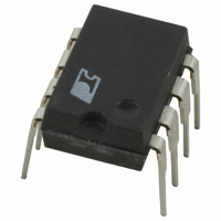
TNY254P Power Integrations, TNY254P Datasheet - Page 7

TNY254P
Manufacturer Part Number
TNY254P
Description
IC OFFLINE SWIT OTP OCP HV 8DIP
Manufacturer
Power Integrations
Series
TinySwitch®r
Datasheet
1.TNY253GN-TL.pdf
(20 pages)
Specifications of TNY254P
Output Isolation
Isolated
Frequency Range
40 ~ 48kHz
Voltage - Output
700V
Power (watts)
4W
Operating Temperature
-40°C ~ 150°C
Package / Case
8-DIP (0.300", 7.62mm)
Output Voltage
5.8 V
Input / Supply Voltage (max)
265 VAC
Input / Supply Voltage (min)
85 VAC
Duty Cycle (max)
68 %
Switching Frequency
44 KHz
Supply Current
140 uA
Operating Temperature Range
- 40 C to + 150 C
Mounting Style
Through Hole
Lead Free Status / RoHS Status
Contains lead / RoHS non-compliant
Available stocks
Company
Part Number
Manufacturer
Quantity
Price
Company:
Part Number:
TNY254P
Manufacturer:
POWER
Quantity:
1 155
Company:
Part Number:
TNY254P
Manufacturer:
POWER
Quantity:
5 510
Part Number:
TNY254P
Manufacturer:
POWER
Quantity:
20 000
Company:
Part Number:
TNY254PN
Manufacturer:
PowerInt
Quantity:
350
Company:
Part Number:
TNY254PN
Manufacturer:
POWER
Quantity:
15 000
Part Number:
TNY254PN
Manufacturer:
POWER
Quantity:
20 000
Figure 12. 0.5 W Open Loop AC Adapter Circuit.
Figure 11. 3.6 W Constant Voltage-Constant Current Cellular Phone Charger Circuit.
constant voltage and constant current output. TinySwitch is
always powered from the input high voltage, therefore it does
not require bias winding for power. Consequently, its operation
is not dependent on the level of the output voltage. This allows
for constant current charger designs that work down to zero
volts on the output.
Figure 11 shows a 5.2 V, 3.6 W cellular phone charger circuit
that uses the TNY254 and provides constant voltage and constant
current output over an universal input (85 to 265 VAC) range.
The AC input is rectified and filtered by D1 - D4, C1 and C2 to
85-265
VAC
1N4005
1N4005
Fusible
D3
115 VAC
10
RF1
D1
15%
1N4005
1N4005
D2
D4
Fusible
1.8
RF1
6.8 F
400 V
C1
1N4004
1N4004
D2
D1
2.2 F
200 V
1.2 k
560 H
4.7 F
400 V
C1
R1
C2
L1
100 k
1 W
R2
100
2.2 F
200 V
R2
C2
TNY254P
68 pF
1 kV
1N4937
C4
2200 pF
U1
D6
C4
D
S
TNY253P
U1
TinySwitch
EN
BP
1
2
create a high voltage DC bus connected to T1 in series with the
high voltage MOSFET inside the TNY254. The inductor L1
forms a π-filter in conjunction with C1 and C2. The resistor R1
damps resonances in the inductor L1. The low frequency of
operation of TNY254 (44 kHz) allows use of the simple π-filter
described above in combination with a single Y1-capacitor C8
to meet worldwide conducted EMI standards. The diode D6,
capacitor C4 and resistor R2 comprise the clamp circuit that
limits the turn-off voltage spike on the TinySwitch DRAIN pin
to a safe value. The secondary winding is rectified and filtered
by D5 and C5 to provide the 5.2 V output. Additional filtering
0.1 F
T1
D
S
LTV817
C3
U2
1
5
EN
BP
10
TinySwitch
5
FR201
T1
Y1 Safety
D5
0.1 F
2.2 nF
2N3904
C3
C8
10
6
Q1
1N3934
D3
47
R9
Y1 Safety
2.2 nF
C5
100 F
1/8 W
16V
18
22
1 W
C6
1
220 F
R4
R5
R3
25 V
C5
100
R7
0.82
1/2 W
R6
1N5239B
VR1
1N5230B
820
3.3 H
TNY253/254/255
220 F
R8
4.7 V
VR1
16 V
L2
C6
+ 9 V
RTN
PI-2244-042303
PI-2190-042303
4/03
+ 5.2 V
RTN
D
7


