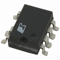
TNY267G Power Integrations, TNY267G Datasheet - Page 7

TNY267G
Manufacturer Part Number
TNY267G
Description
IC OFFLINE SWIT OTP OCP HV 8SMD
Manufacturer
Power Integrations
Series
TinySwitch®-IIr
Datasheet
1.TNY267G.pdf
(24 pages)
Specifications of TNY267G
Output Isolation
Isolated
Frequency Range
124 ~ 140kHz
Voltage - Output
700V
Power (watts)
19W
Operating Temperature
-40°C ~ 150°C
Package / Case
8-SMD Gull Wing, 7 Leads
Lead Free Status / RoHS Status
Contains lead / RoHS non-compliant
Available stocks
Company
Part Number
Manufacturer
Quantity
Price
Company:
Part Number:
TNY267G
Manufacturer:
HARRIS
Quantity:
6 222
Part Number:
TNY267G
Manufacturer:
POWER
Quantity:
20 000
Part Number:
TNY267G-TL
Manufacturer:
POWER
Quantity:
20 000
Company:
Part Number:
TNY267GN
Manufacturer:
POWER
Quantity:
15 000
Part Number:
TNY267GN
Manufacturer:
POWER
Quantity:
20 000
Company:
Part Number:
TNY267GN-TL
Manufacturer:
PowerInt
Quantity:
13 000
Part Number:
TNY267GN-TL
Manufacturer:
POWER
Quantity:
20 000
Figure 14. 2.5 W Constant Voltage, Constant Current Battery Charger with Universal Input (85-265 VAC).
The TinySwitch-II does not require a bias winding to provide
power to the chip, because it draws the power directly from
the DRAIN pin (see Functional Description above). This
has two main benefits. First, for a nominal application, this
eliminates the cost of a bias winding and associated components.
Secondly, for battery charger applications, the current-voltage
characteristic often allows the output voltage to fall close to
zero volts while still delivering power. This type of application
normally requires a forward-bias winding which has many
more associated components. With TinySwitch-II, neither are
necessary. For applications that require a very low no-load power
consumption (50 mW), a resistor from a bias winding to the
BYPASS pin can provide the power to the chip. The minimum
recommended current supplied is 750 µA. The BYPASS pin in
this case will be clamped at 6.3 V. This method will eliminate the
power draw from the DRAIN pin, thereby reducing the no-load
power consumption and improving full-load efficiency.
Current Limit Operation
Each switching cycle is terminated when the DRAIN current
reaches the current limit of the TinySwitch-II. Current limit
operation provides good line ripple rejection and relatively
constant power delivery independent of input voltage.
BYPASS Pin Capacitor
The BYPASS pin uses a small 0.1 µF ceramic capacitor for
decoupling the internal power supply of the TinySwitch-II.
85-265
VAC
1N4005
1N4005
Fusible
8.2 Ω
RF1
D1
D3
1N4005
1N4005
D2
D4
3.3 µF
400 V
C1
2.2 mH
1.2 kΩ
R1
L1
200 kΩ
3.3 µF
R2
400 V
TinySwitch-II
C2
1N4937
TNY264
D6
U1
C3
2.2 nF
D
S
EN/UV
BP
0.1 µF
C3
C8 680 pF
1
4
Y1 Safety
Application Examples
The TinySwitch-II is ideal for low cost, high efficiency power
supplies in a wide range of applications such as cellular phone
chargers, PC standby, TV standby, AC adapters, motor control,
appliance control and ISDN or a DSL network termination.
The 132 kHz operation allows the use of a low cost EE13 or
EF12.6 core transformer while still providing good efficiency.
The frequency jitter in TinySwitch-II makes it possible to use a
single inductor (or two small resistors for under 3 W applications
if lower efficiency is acceptable) in conjunction with two input
capacitors for input EMI filtering. The auto-restart function
removes the need to oversize the output diode for short circuit
conditions allowing the design to be optimized for low cost
and maximum efficiency. In charger applications, it eliminates
the need for a second optocoupler and Zener diode for open
loop fault protection. Auto-restart also saves the cost of adding
a fuse or increasing the power rating of the current sense
resistors to survive reverse battery conditions. For applications
requiring under-voltage lock out (UVLO), such as PC standby,
the TinySwitch-II eliminates several components and saves
cost. TinySwitch-II is well suited for applications that require
constant voltage and constant current output. As
TinySwitch-II is always powered from the input high voltage, it
therefore does not rely on bias winding voltage. Consequently
this greatly simplifies designing chargers that must work down
to zero volts on the output.
T1
LTV817
U2
8
5
1N5819
Shield
2N3904
D5
Q1
10 µF
10 V
47 Ω
C7
R9
1/2 W
1.2 Ω
22 Ω
330 µF
R4
R3
16 V
C5
100 Ω
R7
1/2 W
1 Ω
R6
270 Ω
BZX79-
B3V9
3.9 V
100 µF
R8
TNY263-268
VR1
35 V
C6
PI-2706-080404
4/05
G
500 mA
RTN
+ 5 V
7


