LTC4089EDJC-5#PBF Linear Technology, LTC4089EDJC-5#PBF Datasheet
LTC4089EDJC-5#PBF
Specifications of LTC4089EDJC-5#PBF
Available stocks


Related parts for LTC4089EDJC-5#PBF


LTC4089EDJC-5#PBF Summary of contents
Page 1
... Also featured is programmable total charge time, an NTC thermistor input used to monitor battery temperature while charging and automatic recharging of the battery. L, LT, LTC and LTM are registered trademarks of Linear Technology Corporation. All other trademarks are the property of their respective owners. Protected by U.S. Patents including 6522118, 6700364. ...
Page 2
... LEAD FREE FINISH TAPE AND REEL LTC4089EDJC#PBF LTC4089EDJC#TRPBF LTC4089EDJC-5#PBF LTC4089EDJC-5#TRPBF Consult LTC Marketing for parts specifi ed with wider operating temperature ranges. Consult LTC Marketing for information on non-standard lead based fi nish parts. For more information on lead free part marking, go to: For more information on tape and reel specifi ...
Page 3
ELECTRICAL CHARACTERISTICS temperature range, otherwise specifi cations are at T HPWR = 5V 100k 2k, SUSP = 0V, unless otherwise noted. PROG CLPROG SYMBOL PARAMETER V Input Undervoltage Lockout UVLO dV Input Undervoltage Lockout UVLO Hysteresis ...
Page 4
LTC4089/LTC4089-5 ELECTRICAL CHARACTERISTICS temperature range, otherwise specifi cations are at T HPWR = 5V 100k 2k, SUSP = 0V, unless otherwise noted. PROG CLPROG SYMBOL PARAMETER Internal Ideal Diode R Incremental Resistance, V FWD ON Regulation ...
Page 5
TYPICAL PERFORMANCE CHARACTERISTICS V Load Regulation FLOAT 4. 34k PROG 4.25 4.20 4.15 4.10 4.05 4.00 0 200 400 600 800 I (mA) BAT 40895 G01 Charging from USB BAT BAT 600 ...
Page 6
LTC4089/LTC4089-5 TYPICAL PERFORMANCE CHARACTERISTICS High Voltage Regulator Maximum Load Current 10μH 1.6 1.5 TYPICAL 1.4 1.3 1.2 MINIMUM 1.1 1.0 0 (V) IN 40895 G10 High Voltage Regulator Switch Frequency 800 ...
Page 7
TYPICAL PERFORMANCE CHARACTERISTICS Input Connect Waveforms V IN 5V/DIV V OUT 5V/DIV I IN 0.5A/DIV I BAT 0.5A/DIV 40895 G18 1ms/DIV V = 3.85V BAT I = 100mA OUT Wall Connect Waveforms WALL 5V/DIV V OUT 5V/DIV I WALL 0.5A/DIV ...
Page 8
LTC4089/LTC4089-5 PIN FUNCTIONS GND (Pins 1, 2): Ground. Tie the GND pin to a local ground plane below the LTC4089 and the circuit components. HVOUT (Pins 3, 18): Voltage Output of the High Voltage Regulator. When suffi cient voltage is ...
Page 9
PIN FUNCTIONS OUT (Pin 13): Voltage Output. This pin is used to provide controlled power to a USB device from either USB V (IN), an external high voltage supply (HVIN), or the battery (BAT) when no other supply is present. ...
Page 10
LTC4089/LTC4089-5 BLOCK DIAGRAM HVIN 10 + – OSCILLATOR 10pF ENABLE R3 HVEN 1000 CURRENT CONTROL CL CLPROG – 500mA/100mA HPWR 13 2μ CHG – PROG ...
Page 11
... Input Current Limit Whenever the input power path is enabled (i.e., SUSP = 0V and HVIN = 0V) and power is available at IN, power is delivered to OUT. The current limit and charger control circuits of the LTC4089/LTC4089-5 are designed to limit PowerPath is a trademark of Linear Technology Corporation. Q1 HIGH VOLTAGE BUCK REGULATOR + 4.25V (RISING) – ...
Page 12
LTC4089/LTC4089-5 OPERATION input current as well as control battery charge current as a function The input current limit, I OUT programmed using the following formula: ⎡ ⎤ 1000 = ⎥ • V ⎢ CL CLPROG ...
Page 13
OPERATION High Voltage Step Down Regulator The power delivered from HVIN to HVOUT is controlled by a 750kHz constant frequency, current mode step down regulator. An external P-channel MOSFET directs this power to OUT and prevents reverse conduction from OUT ...
Page 14
LTC4089/LTC4089-5 OPERATION then no external components are necessary. However, if more conductance is needed, an external P-channel MOSFET can be added from BAT to OUT. The GATE pin of the LTC4089/LTC4089-5 drives the gate of the PFET for automatic ideal ...
Page 15
OPERATION when the LTC4089/LTC4089-5 is powered from the IN pin, the programmed input current limit takes precedent over the charge current. In such a scenario, the charge current cannot exceed the programmed input current limit. For example, if typical 500mA ...
Page 16
LTC4089/LTC4089-5 OPERATION If, for some reason the charge current rises back above the threshold, the CHRG pin will not resume the strong pull-down state. The EOC latch can be reset by a recharge cycle (i.e., V drops below the recharge ...
Page 17
APPLICATIONS INFORMATION USB and 5V Wall Adapter Power Although the LTC4089/LTC4089-5 is designed to draw power from a USB port, a higher power 5V wall adapter can also be used to power the application and charge the battery (higher voltage ...
Page 18
LTC4089/LTC4089-5 APPLICATIONS INFORMATION The high voltage regulator output capacitor controls output ripple, supplies transient load currents, and stabilizes the regulator control loop. Ceramic capacitors have very low equivalent series resistance (ESR) and provide the best ripple performance. A good value ...
Page 19
APPLICATIONS INFORMATION Increasing R will move both trip points to lower NOM temperatures. Likewise, a decrease will move the trip points to higher temperatures. NTC To calculate R for a shift to lower temperature, for NOM ...
Page 20
LTC4089/LTC4089-5 APPLICATIONS INFORMATION Power Dissipation and High Temperature Considerations The die temperature of the LTC4089/LTC4089-5 must be lower than the maximum rating of 110°C. This is generally not a concern unless the ambient temperature is above 85°C. The total power ...
Page 21
APPLICATIONS INFORMATION The power dissipation in the other power compo- nents—catch diodes, MOSFETs, boost diodes and induc- tors—causes additional copper heating and can further increase the “ambient” temperature of the IC. Board Layout Considerations As discussed in the previous section, ...
Page 22
LTC4089/LTC4089-5 APPLICATIONS INFORMATION 36V 22μF 1M GND 50V 1% JP1 VIN 1000pF OFF 50V E3 USB 4.35V C5 TO 5.5V 4.7μF 6.3V JP2 CURRENT ...
Page 23
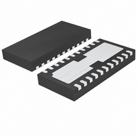
... SHADED AREA IS ONLY A REFERENCE FOR PIN 1 LOCATION ON TOP AND BOTTOM OF PACKAGE Information furnished by Linear Technology Corporation is believed to be accurate and reliable. However, no responsibility is assumed for its use. Linear Technology Corporation makes no representation that the interconnection of its circuits as described herein will not infringe on existing patent rights. LTC4089/LTC4089-5 DJC Package 22-Lead Plastic DFN (6mm × ...
Page 24
... USB Power Controller and Li-Ion Battery Charger with Low-Loss Ideal Diode LTC4085 USB Power Manager with Ideal Diode Controller and Li-Ion Charger ThinSOT is a trademark of Linear Technology Corporation. Linear Technology Corporation 24 1630 McCarthy Blvd., Milpitas, CA 95035-7417 (408) 432-1900 FAX: (408) 434-0507 ● ...