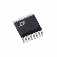
LTC4006EGN-2 Linear Technology, LTC4006EGN-2 Datasheet - Page 8

LTC4006EGN-2
Manufacturer Part Number
LTC4006EGN-2
Description
IC CHARGER BATTERY 4A 16-SSOP
Manufacturer
Linear Technology
Datasheet
1.LTC4006EGN-2PBF.pdf
(20 pages)
Specifications of LTC4006EGN-2
Function
Charge Management
Battery Type
Lithium-Ion (Li-Ion)
Voltage - Supply
6 V ~ 28 V
Operating Temperature
-40°C ~ 85°C
Mounting Type
Surface Mount
Package / Case
16-SSOP (0.150", 3.90mm Width)
Output Current
4A
Output Voltage
12.6V
Operating Supply Voltage (min)
6V
Operating Supply Voltage (max)
28V
Operating Temp Range
-40C to 85C
Package Type
SSOP N
Mounting
Surface Mount
Pin Count
16
Operating Temperature Classification
Industrial
Lead Free Status / RoHS Status
Contains lead / RoHS non-compliant
Lead Free Status / RoHS Status
Contains lead / RoHS non-compliant
Available stocks
Company
Part Number
Manufacturer
Quantity
Price
Company:
Part Number:
LTC4006EGN-2
Manufacturer:
LT
Quantity:
10 000
Part Number:
LTC4006EGN-2
Manufacturer:
LINEAR/凌特
Quantity:
20 000
Part Number:
LTC4006EGN-2#PBF
Manufacturer:
LINEAR/凌特
Quantity:
20 000
OPERATIO
LTC4006
Overview
The LTC4006 is a synchronous current mode PWM step-
down (buck) switcher battery charger controller. The charge
current is programmed by the sense resistor (R
between the CSP and BAT pins. The final float voltage is
internally programmed to 8.4V (LTC4006-6), 12.6V
(LTC4006-2) or 16.8V (LTC4006-4) with better than ±0.8%
accuracy. Charging begins when the potential at the DCIN
pin rises above the voltage at CLN (and the UVLO voltage)
and the ACP/SHDN pin is allowed to go high; the CHG pin
is set low. At the beginning of the charge cycle, if the cell
voltage is below 2.5V, the charger will trickle charge the
battery with 10% of the maximum programmed current.
If the cell voltage stays below 2.5V for 25% of the total
charge time, the charge sequence will be terminated im-
mediately and the CHG pin will be set to a high impedance.
An external thermistor network is sampled at regular
intervals. If the thermistor value exceeds design limits,
charging is suspended. If the thermistor value returns to
an acceptable value, charging resumes. An external resis-
tor on the R
be defeated by forcing the CHG pin to a low voltage.
As the battery approaches the final float voltage, the charge
current will begin to decrease. When the current drops to
10% of the programmed charge current, an internal C/10
comparator will indicate this condition by sinking 25µA at the
CHG pin. The charge timer is also reset to 25% of the total
charge time. If this condition is caused by an input current
limit condition, described below, then the C/10 comparator
will be inhibited. When a time-out occurs, charging is termi-
nated immediately and the CHG pin changes to a high
impedance. The charger will automatically restart if the cell
voltage is less than 3.9V. To restart the charge cycle manu-
ally, simply remove the input voltage and reapply it, or force
the ACP/SHDN pin low momentarily. When the input voltage
is not present, the charger goes into a sleep mode, dropping
battery current drain to 15µA. This greatly reduces the current
drain on the battery and increases the standby time. The
charger can be inhibited at any time by forcing the ACP/SHDN
pin to a low voltage.
Input FET
The input FET circuit performs two functions. It enables
the charger if the input voltage is higher than the CLN pin
and provides the logic indicator of AC present on the
8
T
pin sets the total charge time. The timer can
U
SENSE
)
ACP/SHDN pin. It controls the gate of the input FET to keep
a low forward voltage drop when charging and also
prevents reverse current flow through the input FET.
If the input voltage is less than V
170mV higher than V
occurs the ACP/SHDN pin is released and pulled up with
an internal load to indicate that the adapter is present. The
gate of the input FET is driven to a voltage sufficient to keep
a low forward voltage drop from drain to source. If the
voltage between DCIN and CLN drops to less than 25mV,
the input FET is turned off slowly. If the voltage between
DCIN and CLN is ever less than – 25mV, then the input FET
is turned off in less than 10µs to prevent significant
reverse current from flowing in the input FET. In this
condition, the ACP/SHDN pin is driven low and the charger
is disabled.
Battery Charger Controller
The LTC4006 charger controller uses a constant off-time,
current mode step-down architecture. During normal opera-
tion, the top MOSFET is turned on each cycle when the
oscillator sets the SR latch and turned off when the main
current comparator I
MOSFET is off, the bottom MOSFET is turned on until either
the inductor current trips the current comparator I
beginning of the next cycle. The oscillator uses the equation:
to set the bottom MOSFET on time. This activity is dia-
grammed in Figure 1.
The peak inductor current, at which I
is controlled by the voltage on I
several loops, depending upon the situation at hand. The
average current control loop converts the voltage between
CSP and BAT to a representative current. Error amp CA2
t
OFF
TGATE
BGATE
INDUCTOR
CURRENT
=
OFF
OFF
ON
ON
V
V
DCIN
DCIN
–
•
V
f
OSC
BAT
CMP
CLN
TRIP POINT SET BY ITH VOLTAGE
to activate the charger. When this
resets the SR latch. While the top
Figure 1
t
OFF
TH
. I
TH
CLN
CMP
is in turn controlled by
, it must go at least
resets the SR latch,
4006 F01
REV
or the
4006fa


