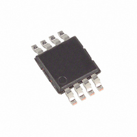
DS2740BU+ Maxim Integrated Products, DS2740BU+ Datasheet

DS2740BU+
Specifications of DS2740BU+
Related parts for DS2740BU+
DS2740BU+ Summary of contents
Page 1
FEATURES 15-Bit Bidirectional Current Measurement (DS2740U) 1.56μV LSB and ±51.2mV Dynamic Range 78μA LSB and ±2.56A Dynamic Range with External 20mΩ Sense Resistor (R ) SNS 156μA LSB and ±5.12A Dynamic Range with External 10mΩ Sense Resistor (R ) ...
Page 2
... D2740 (see note) DS2740BU DS2740BU+ 2740B (see note) DS2740BU/T&R DS2740BU+T&R 2740B (see note) Note: A “+” will also be marked on the package next to the pin 1 indicator. DESCRIPTION The DS2740 provides high-precision current-flow measurement data to support battery-capacity monitoring in cost-sensitive applications. Current is measured bidirectionally over a dynamic range of 15 bits (DS2740U bits (DS2740BU), with the net flow accumulated in a separate 16-bit register ...
Page 3
Figure 1. BLOCK DIAGRAM V DD 1-WIRE DQ INTERFACE AND ADDRESS SNS STATUS/CONTROL ACCUMULATED CURRENT CURRENT 15-Bit + Sign ADC Ω Ω IS2 IS1 R SNS PIO TIMEBASE ...
Page 4
Table 2. DETAILED PIN DESCRIPTIONS PIN SYMBOL 1-Wire Bus Speed Control. Input logic level selects the speed of the 1- Wire bus. Logic 1 selects overdrive (OVD) and Logic 0 selects standard OVD 1 timing (STD multidrop bus, ...
Page 5
POWER MODES The DS2740 has two power modes: Active and Sleep. While in Active mode, the DS2740 operates as a high-precision coulomb counter with current and accumulated current measurement blocks operating continuously and the resulting values updated in the measurement ...
Page 6
CONVERSION PART TIME DS2740U 3.515s DS2740BU 0.878s Every 1024th conversion, the ADC measures its input offset to facilitate offset correction. Offset correction occurs approximately once per hour in the DS2740U and four times per hour in the DS2740BU. The resulting ...
Page 7
PART V IS1 DS2740U ±204.8mVh DS2740BU MEMORY The DS2740 has memory space with registers for instrumentation, status, and control. When the MSB of a two-byte register is read, both the MSB and LSB are latched and held for the duration ...
Page 8
SPECIAL FEATURE REGISTER The format of the special feature register is shown in Figure 6. The function of each bit is described in detail in the following paragraphs. Figure 6. SPECIAL FEATURE REGISTER FORMAT BIT 7 BIT 6 X PIO ...
Page 9
The CRC can be generated by the host using a circuit consisting of a shift register and XOR gates as shown in Figure can be generated in software. Additional information about the Dallas 1-Wire CRC is available ...
Page 10
Figure 9. 1-Wire BUS INTERFACE CIRCUITRY BUS MASTER Rx Tx TRANSACTION SEQUENCE The protocol for accessing the DS2740 through the 1-Wire port is as follows: Initialization Net Address Command Function Command Transaction/Data The sections that follow describe each of these ...
Page 11
Skip Net Address [CCh]. This command saves time when there is only one DS2740 on the bus by allowing the bus master to issue a function command without specifying the address of the slave. If more than one slave device ...
Page 12
Figure 10. NET ADDRESS COMMAND FLOW CHART 33h / 39h NO READ MATCH YES MASTER Tx DS2740 Tx BIT 0 FAMILY CODE 1 BYTE DS2740 Tx SERIAL NUMBER 6 BYTES MATCH ? DS2740 Tx CRC 1 BYTE MASTER Tx BIT ...
Page 13
Table 4. FUNCTION COMMANDS COMMAND DESCRIPTION Reads data from Read Data memory starting at address XX Writes data to memory Write Data starting at address XX 1-Wire SIGNALING The 1-Wire bus requires strict signaling protocols to ensure data integrity. The ...
Page 14
READ-TIME SLOTS A read-time slot is initiated when the bus master pulls the 1-Wire bus line from a logic-high level to a logic-low level. The bus master must keep the bus line low for at least 1 DS2740 to present ...
Page 15
ABSOLUTE MAXIMUM RATINGS* Voltage DQ, IS1, IS2, PIO, Relative Voltage on SNS, Relative to V Operating Temperature Range Storage Temperature Range Soldering Temperature * This is a stress rating only and functional operation of ...
Page 16
Input Logic Low: DQ, PIO Output Logic Low: DQ, PIO DQ, PIO Input Pulldown Current OVD Input Leakage IL DQ Capacitance DQ Low to Sleep Time t ELECTRICAL CHARACTERISTICS: 1-Wire INTERFACE—STANDARD SPEED (2.7V ≤ V ≤ 5.5V ...


