ADE7751ARS Analog Devices Inc, ADE7751ARS Datasheet
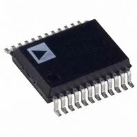
IC ENERGY METERING DETEC 24-SSOP

ADE7751ARS

Manufacturer Part Number
ADE7751ARS
Description
IC ENERGY METERING DETEC 24-SSOP
Manufacturer
Analog Devices Inc
Datasheet

Specifications of ADE7751ARS

Rohs Status
RoHS non-compliant
Input Impedance
390 KOhm
Measurement Error
0.1%
Voltage - I/o High
2.4V
Voltage - I/o Low
0.8V
Current - Supply
3mA
Voltage - Supply
4.75 V ~ 5.25 V
Operating Temperature
-40°C ~ 85°C
Mounting Type
Surface Mount
Package / Case
24-SSOP (0.200", 5.30mm Width)
Meter Type
Single Phase
For Use With
EVAL-ADE7751ZEB - BOARD EVALUATION FOR ADE7751
Lead Free Status / RoHS Status
Not Compliant

Available stocks

Company
Part Number
Manufacturer
Quantity
Price
Part Number:
ADE7751ARS
Manufacturer:
AD
Quantity:
43
Part Number:
ADE7751ARS
Manufacturer:
ADI/亚德诺
Quantity:
20 000
Part Number:
ADE7751ARSZ
Manufacturer:
ST
Quantity:
6 219
Part Number:
ADE7751ARSZ
Manufacturer:
ADI/亚德诺
Quantity:
20 000
Part Number:
ADE7751ARSZRL
Manufacturer:
AD
Quantity:
1 450
a
GENERAL DESCRIPTION
The ADE7751 is a high-accuracy, fault-tolerant electrical energy
measurement IC that is intended for use with 2-wire distribution
systems. The part specifications surpass the accuracy require-
ments as quoted in the IEC1036 standard.
Information furnished by Analog Devices is believed to be accurate and
reliable. However, no responsibility is assumed by Analog Devices for its
use, nor for any infringements of patents or other rights of third parties that
may result from its use. No license is granted by implication or otherwise
under any patent or patent rights of Analog Devices.
*US Patent 5,745,323; 5,760,617; 5,862,069; 5,872,469.
REV. 0
FEATURES
High Accuracy, Surpasses 50 Hz/60 Hz IEC 687/1036
Less than 0.1% Error over a Dynamic Range of 500 to 1
Supplies Average Real Power on the Frequency
High-Frequency Output CF Is Intended for Calibration
Continuous Monitoring of the Phase and Neutral
ADE7751 Uses the Larger of the Two Currents (Phase
Two Logic Outputs (FAULT and REVP) Can Be Used to
Direct Drive for Electromechanical Counters and
A PGA in the Current Channel Allows the Use of Small
Proprietary ADCs and DSP Provide High Accuracy over
On-Chip Power Supply Monitoring
On-Chip Creep Protection (No Load Threshold)
On-Chip Reference 2.5 V
Single 5 V Supply, Low Power (15 mW Typical)
Low-Cost CMOS Process
Outputs F1 and F2
and Supplies Instantaneous Real Power
Current Allows Fault Detection in 2-Wire
Distribution Systems
or Neutral) to Bill—Even During a Fault Condition
Indicate a Potential Miswiring or Fault Condition
2-Phase Stepper Motors (F1 and F2)
Values of Shunt and Burden Resistance
Large Variations in Environmental Conditions and Time
with External Overdrive Capability
V1A
V1N
V1B
V2P
V2N
8% (30 ppm/ C Typical)
G0 G1
REFERENCE
1,
1,
2.5V
PGA
2,
FUNCTIONAL BLOCK DIAGRAM
PGA
2,
SUPPLY MONITOR
8,
8,
AV
REF
4k
POWER
16
16
DD
ADC
ADC
ADC
IN/OUT
AGND
...
...
...
CLKIN
110101
110101
11011001
CLKOUT
...
...
One Technology Way, P.O. Box 9106, Norwood, MA 02062-9106, U.S.A.
Tel: 781/329-4700
Fax: 781/326-8703
The only analog circuitry used in the ADE7751 is in the ADCs
and reference circuit. All other signal processing (e.g., multipli-
cation and filtering) is carried out in the digital domain. This
approach provides superior stability and accuracy over extremes
in environmental conditions and over time.
The ADE7751 incorporates a novel fault detection scheme that
warns of fault conditions and allows the ADE7751 to continue
accurate billing during a fault event. The ADE7751 does this
by continuously monitoring both the phase and neutral (return)
currents. A fault is indicated when these currents differ by more
than 12.5%. Billing is continued using the larger of the two currents.
The ADE7751 supplies average real power information on the
low-frequency outputs F1 and F2. These logic outputs may be
used to directly drive an electromechanical counter or interface
to an MCU. The CF logic output gives instantaneous real power
information. This output is intended to be used for calibration purposes.
The ADE7751 includes a power supply monitoring circuit on the
AV
until the supply voltage on AV
below 4 V, the ADE7751 will also be reset and no pulses will be
issued on F1, F2, and CF.
Internal phase matching circuitry ensures that the voltage and
current channels are matched whether the HPF in Channel 1 is
on or off. The ADE7751 also has anticreep protection.
The ADE7751 is available in 24-lead DIP and SSOP packages.
...
FAULT
A
B
A<>B
A>B
B>A
DD
DIGITAL-TO-FREQUENCY
SCF S0 S1
ADE7751
with On-Chip Fault Detection
supply pin. The ADE7751 will remain in a reset condition
PHASE
CORRECTION
CONVERTER
AC/DC
REVP
HPF
PROCESSING
CF
DV
SIGNAL
BLOCK
MULTIPLIER
DD
F1 F2
DGND
Energy Metering IC
RESET
LPF
DD
reaches 4 V. If the supply falls
© Analog Devices, Inc., 2002
ADE7751
www.analog.com
*

Related parts for ADE7751ARS

ADE7751ARS Summary of contents

Page 1

FEATURES High Accuracy, Surpasses 50 Hz/60 Hz IEC 687/1036 Less than 0.1% Error over a Dynamic Range of 500 to 1 Supplies Average Real Power on the Frequency Outputs F1 and F2 High-Frequency Output CF Is Intended for Calibration ...

Page 2

ADE7751–SPECIFICATIONS Parameter 3 ACCURACY 1 Measurement Error on Channels 1 and 2 Gain = 1 Gain = 2 Gain = 8 Gain = 16 1 Phase Error between Channels V1 Phase Lead 37 (PF = 0.8 Capacitive) V1 Phase Lag ...

Page 3

Parameter 4 LOGIC OUTPUTS F1 and F2 Output High Voltage Output Low Voltage CF, FAULT, and REVP Output High Voltage Output Low Voltage POWER SUPPLY ...

Page 4

... Therefore, proper ESD precautions are recommended to avoid performance degradation or loss of functionality. ORDERING GUIDE Model Package Description ADE7751AN Plastic DIP ADE7751ARS Shrink Small Outline Package RS-24 ADE7751ARSRL Shrink Small Outline Package RSRL- Reel EVAL-ADE7751EB ADE7751 Evaluation Board + 0.3 V ...

Page 5

Pin No. Mnemonic Description 1 DV Digital Power Supply. This pin provides the supply voltage for the digital circuitry in the ADE7751. DD The supply voltage should be maintained decoupled with capacitor in parallel ...

Page 6

ADE7751 Pin No. Mnemonic Description 13, 14 S1, S0 These logic inputs are used to select one of four possible frequencies for the digital-to-frequency conversion. This offers the designer greater flexibility when designing the energy meter. See Select- ing a ...

Page 7

0.40 GAIN = 1 ON-CHIP REFERENCE 0.30 +85 C 0.20 0.10 –40 C 0.00 –0.10 –0.20 –0.30 –0.40 –0.50 0.01 0.10 1.00 AMPS TPC 1. Error Reading (Gain = 1) 0.25 PF ...

Page 8

ADE7751 0.20 +25 C PF=1 0.10 0.00 +85 C PF=0.5 –0.10 –0.20 +25 C PF=0.5 –0.30 –0.40 –0. 0.5 GAIN = 8 ON-CHIP REFERENCE –0.60 0.01 0.1 1 AMPS TPC 7. Error Reading (PF ...

Page 9

TPC 13. Channel 1 Offset Distribution (Gain = TPC 14. Channel 1 Offset ...

Page 10

ADE7751 THEORY OF OPERATION The two ADCs digitize the voltage and current signals from the current and voltage transducers. These ADCs are 16-bit second order sigma-delta converters with an oversampling rate of 900 kHz. This analog input structure greatly simplifies ...

Page 11

Using Equations 2 and 3, the real power P can be expressed in terms of its fundamental real power (P power ( where cos ...

Page 12

ADE7751 Figure 7 shows two typical connections for Channel V2. The first option uses a PT (potential transformer) to provide complete isola- tion from the mains voltage. In the second option, the ADE7751 is biased around the neutral wire and ...

Page 13

FREQUENCY – Hz Figure 11. Phase Error Between Channels ( Hz) DIGITAL-TO-FREQUENCY CONVERSION As previously described, the digital output of the low-pass filter after ...

Page 14

ADE7751 V1A V1A V1B V1A AGND V1N 0V V1B V1B V1B < 87.5% OF V1A Figure 13. Fault Conditions for Inactive Input Less than Active Input Fault with V1B Greater than V1A Figure 14 illustrates another fault condition. If V1A ...

Page 15

Example 1 If full-scale differential dc voltages of +660 mV and –660 mV are applied to V1 and V2 respectively (660 mV is the maximum differential voltage that can be connected to Channel 1 and Channel 2), the expected output ...

Page 16

ADE7751 When selecting a suitable F frequency for a meter design, the 1–4 frequency output at I (maximum load) with a meter constant MAX of 100 imp/kWhr should be compared with Column 4 of Table VI. The frequency that is ...

Related keywords