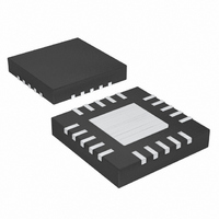
MAX3656ETG+T Maxim Integrated Products, MAX3656ETG+T Datasheet - Page 9

MAX3656ETG+T
Manufacturer Part Number
MAX3656ETG+T
Description
IC LASR DRVR 2.5GBPS 3.6V 24TQFN
Manufacturer
Maxim Integrated Products
Type
Laser Diode Driver (Fiber Optic)r
Datasheet
1.MAX3656ETG.pdf
(15 pages)
Specifications of MAX3656ETG+T
Data Rate
2.5Gbps
Number Of Channels
1
Voltage - Supply
3 V ~ 3.6 V
Current - Supply
40mA
Current - Modulation
85mA
Current - Bias
70mA
Operating Temperature
-40°C ~ 85°C
Package / Case
24-TQFN Exposed Pad
Mounting Type
Surface Mount
Lead Free Status / RoHS Status
Lead free / RoHS Compliant
Other names
MAX3656ETG+T
MAX3656ETG+TTR
MAX3656ETG+TTR
The MAX3656 laser driver has three main parts: a high-
speed modulator, a high-speed bias driver, and a laser-
biasing block with automatic power control (see the
Functional Diagram ). Both the bias and modulation output
stages are composed of differential pairs with program-
mable current sources. The circuit design is optimized for
high-speed, low-voltage (3.3V), DC-coupled operation.
The device is ideal for burst-mode operation with turn-on
and turn-off times less than 2ns. The MAX3656 can be
configured for nonburst-mode applications (continuous
mode) by connecting BEN high.
To maintain constant average optical power, the
MAX3656 incorporates a digital automatic power-con-
trol (APC) loop to compensate for the changes in laser
threshold current over temperature and lifetime. A
back-facet photodiode mounted in the laser package
converts the optical power into a photocurrent. The
APC loop adjusts the laser bias current so the monitor
current is matched to a reference current set by R
At startup, the APC loop traverses through a pseudo-
binary search algorithm to set the proper monitor current
that translates to the proper bias current. When BEN is
high, the APC loop maintains constant optical power by
digitally controlling the bias current. When BEN is low,
the APC loop digitally stores the bias current value of the
previous burst. The APC loop is reset in two ways, either
power cycling or toggling the EN pin.
An external resistor (R
able bias current during closed-loop operation and sets
the bias current during open-loop operation. An APC fail-
ure flag (FAIL) is set low during initialization and when
the bias current cannot be adjusted to achieve the
desired average optical power.
APC closed-loop operation requires that the user set
three currents with external resistors connected between
GND, BIASMAX, MODSET, and APCSET pins. Detailed
guidelines for these resistor settings are described in the
Design Procedure section.
If necessary, the MAX3656 is fully operational without
APC. To operate the MAX3656 open loop, connect a
50kΩ resistor from APCSET to ground and leave the
MD pin unconnected. In this case, two external resis-
tors connected from BIASMAX and MODSET to GND
directly set the laser current.
The MAX3656 provides an APC failure monitor (TTL) to
indicate an APC loop-tracking failure. FAIL is set low
when the APC loop cannot adjust the bias current to
_______________________________________________________________________________________
BIASMAX
Detailed Description
Automatic Power Control
APC Failure Monitor
) sets the maximum allow-
155Mbps to 2.5Gbps Burst-Mode
APCSET
.
maintain the desired monitor current. For example, the
laser diode requires more bias current (to maintain a
constant optical output) than maximum bias current set
by R
asserted. In an alternate example, assume that a circuit
failure causes the cathode of the laser diode to be short-
ed to GND, thereby causing an uncontrolled high optical
output. In this case, the APC loop cannot decrease the
user current, and FAIL is asserted. FAIL is also set low
during initialization.
For safety reasons, at initial power-up or after toggling
EN, the MAX3656 incorporates a slow-start circuit that
provides a typical delay of 450ns during the beginning
of APC loop initialization.
The MAX3656 features a chip-enable function. When
EN is high, the bias and modulation currents are off and
the digital state of the APC loop is reset. When EN is
toggled from a high to a low, the APC loop begins ini-
tialization. The initialization time is typically 2.1µs
(LONGB = low) and 3.72µs (LONGB = high).
The digital APC loop is reset whenever the power is
turned off and/or the EN input is driven high. When
power is turned on or when EN is toggled low, the APC
loop automatically performs an initialization routine that
quickly adjusts the bias current from its reset level to its
initialized level. The initialized bias current level is
defined to be within 3.8mA of the final bias current level
set by the APCSET resistor. Once initialized, the APC
loop enters its fine-adjustment mode of operation and
adjusts the bias current to match the level set by the
APCSET resistor. There are three different cases in
which the APC loop starts initialization, and each has a
unique initialization time. These cases are defined
as follows:
•
•
Continuous-Mode Power-Up
In continuous-mode power-up, the chip is enabled
(EN = low) and the burst-enable input is high (BEN =
high) when power is applied to the laser driver. APC
loop initialization begins when the power-supply volt-
age rises above the minimum specified limit of +3.0V.
The BEN input remains high indefinitely and the laser
driver operates in continuous (nonbursting) mode. In
this case, the initialization time is 12µs (typ).
Chip-Enable Reset
In chip-enable reset, the power-supply voltage is
within the specified limits and BEN is high. The chip-
enable input (EN) is initially high (chip disabled and
BIASMAX
. The bias current is limited and FAIL is
Laser Driver
APC Loop Initialization
Enable Control
Slow-Start
9


