LX1689CPW Microsemi Analog Mixed Signal Group, LX1689CPW Datasheet
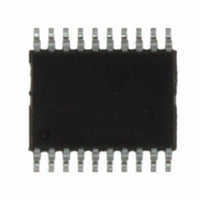
IC CTRLR CCFL BACKLIGHT 20TSSOP

LX1689CPW

Manufacturer Part Number
LX1689CPW
Description
IC CTRLR CCFL BACKLIGHT 20TSSOP
Manufacturer
Microsemi Analog Mixed Signal Group
Type
CCFL Controllerr
Datasheet

Specifications of LX1689CPW

Frequency
63 ~ 67 kHz
Current - Supply
5.5mA
Current - Output
100mA
Voltage - Supply
3 V ~ 28 V
Operating Temperature
0°C ~ 70°C
Package / Case
20-TSSOP
Lead Free Status / RoHS Status
Lead free / RoHS Compliant

Available stocks

Company
Part Number
Manufacturer
Quantity
Price
Part Number:
LX1689CPW
Manufacturer:
MICRO
Quantity:
1 505
Part Number:
LX1689CPW
Manufacturer:
ST
0
Part Number:
LX1689CPW
Manufacturer:
MSC
Quantity:
20 000
Company:
Part Number:
LX1689CPW-TR
Quantity:
2 500
Part Number:
LX1689CPWTR
Manufacturer:
SONY
Quantity:
322
Copyright © 2000
Rev. 1.1, 2006-02-27
Direct Drive CCFL (Cold Cathode
Fluorescent Lamp) Controller. It uses
new circuit design techniques (patents
pending) and combines digital and linear
circuits with an advanced BiCMOS
process to create a more complete
controller in a small package.
LX1686
applications use from 12 to 30 less
components.
enhancements have been added to make
the LX1689 even easier to use.
synchronize the digital dimming burst
frequency to the video frame rate, as
used in the LX1686, is replaced with a
programmable counter. This counter can
divide the video controller horizontal
sync pulse, other external clock source
or the internal chip clock source to
generate the burst frequency.
IMPORTANT: For the most current data, consult MICROSEMI’s website:
Protected By U.S. Patents: 5,615,093; 5,923,129; 5,930,121; 6,198,234; Patents Pending
*As Shown in Figure 1 (Typical Application)
The LX1689 is the latest generation
When compared to the original
The on-chip PLL circuit used to
TM
Actual Inverter Size
design,
New
Note: Available in Tape & Reel. Append the letters “TR” to the part number. (i.e. LX1689CPW-TR)
-40 to 85
identical
0 to 70
T
11861 Western Avenue, Garden Grove, CA. 92841, 714-898-8121, Fax: 714-893-2570
1.38in.
J
functions
(°C)
2.64in.
Actual Inverter Size
OR
(35mm)
D E S C R I P T I O N
(67mm)
module
LX1689 CCFL Inverter Layouts Examples*
and
M
.870 in.
(22mm)
IN
use of either a DC voltage or a PWM
input to simplify design. Programmable
polarity brightness control is retained,
except in the case of externally clocked
digital dimming.
regulators extend the input voltage range
of the IC up to 28 Volts without using
external circuitry as was required with our
previous
includes a new lamp strike detection
scheme that saves a package pin and three
external components.
monitor lamp current pulses at the I_SNS
input to determine if the lamp strikes and
if it stays ignited once operational.
each of three lamp inputs has significantly
reduced the lamp feedback component
count. In addition the controller features
include auto shutdown for open or broken
lamps, and a lamp fault detection with a
status reporting output.
3V
3V
V
P R O D U C T H I G H L I G H T
The brightness control input allows the
DD
Integrating full wave rectifiers for
P A C K A G E O R D E R I N F O
Integrated Products
®
http://www.microsemi.com
Microsemi
controllers.
.397 in
(10mm)
M
.
AX
28V
28V
Two onboard LDO
V
DD
Third Generation CCFL Controller
Internal circuits
The
RoHS Compliant / Pb-free Transition DC: 0442
PW
P
LX1689
RODUCTION
Plastic TSSOP
20-PIN
21
LX1689CPW
LX1689IPW
1
1
1
2
7
9
Bill of Materials
D
ATA
3 to 28 Volt Single Fixed (±20%)
Supply Operating Range
Selectable Analog/Digital
Dimming Modes
Digital Dimming Can Synch to
External Or Internal Clocks
User Programmable Digital
Dimming Burst Frequency
252 mS Power On Delay
Flexible Lamp Current
Compensation Input
Open Lamp Shutdown and Fault
Output Indicator
“On Chip” Full Wave Lamp
Current & Voltage Rectifiers
20 Pin TSSOP Package
Low Component Count /
Module Cost / Size
High “Nits/Watt” Efficiency
Operates Directly From 1 to 6
Li_Ion Cells
Lamp Current Compensation
Input Makes Indoor/Outdoor
And Wide Temperature Range
Applications Easy to Design
LX1689CPW
K E Y F E A T U R E S
Transformer
Total Count
Connectors
Capacitors
Dual FET
S
Resistors
HEET
B E N E F I T S
LX1689
Page 1

Related parts for LX1689CPW

LX1689CPW Summary of contents

Page 1

... Shown in Figure 1 (Typical Application) T (° - Note: Available in Tape & Reel. Append the letters “TR” to the part number. (i.e. LX1689CPW-TR) Copyright © 2000 Rev. 1.1, 2006-02-27 11861 Western Avenue, Garden Grove, CA. 92841, 714-898-8121, Fax: 714-893-2570 Third Generation CCFL Controller ® ...

Page 2

Supply Voltage ( )................................................................................................. 30V V _BATT Digital Input ( ).....................................................................................-0. ENABLE Analog Inputs Transient ...

Page 3

AME Digital Dimming Clock / Dimming Polarity. An input pin that may ...

Page 4

AME BRITE Filter Capacitor and FAULT Output. Used to convert higher frequency ...

Page 5

... BRITE_IN Linear DC Voltage Range BRITE_IN PWM Logic Signal Voltage Range Digital Inputs (DIM_MODE, DIV_248,DIM_CLK) Maximum Output Gate Charge ( OUT Unless otherwise specified, the following specifications apply over the operating ambient temperature: LX1689CPW: 0 ° C ≤ ≤ LX1689IPW: -40°C T 85°C, except where otherwise noted. ...

Page 6

Parameter RAMP GENERATOR ...

Page 7

Parameter ANALOG DIMMER ...

Page 8

TM V_BATT ENABLE & BIAS ENABLE SLEEP SHUTDOW N VDD_A DUAL LDO VDD_P UVLO BIAS I_R BRITE_IN 2. 75K 0.5V VDD_A FAULT BRITE_C ANADIM BRITE_O UT VDD_A BRITE_R - + I 1 DIM _CLK DIM ...

Page 9

... DIV_248 I_SNS BRITE_C BRITE_OUT C2 100nF 16V BRITE_R EA_OUT 6.65 BRITE_IN EA_IN ENABLE I_R LX1689CPW F 2 – LX1689 Typical 1W Application IGURE DIM_CLK DIMMING MODE External Burst External Clock Source Dimming from divided DIM_CLK input VDD_A Analog Dimming GND Analog Dimming Internal Burst ...

Page 10

TM Copyright © 2000 Rev. 1.1, 2006-02-27 11861 Western Avenue, Garden Grove, CA. 92841, 714-898-8121, Fax: 714-893-2570 Third Generation CCFL Controller ® – Typical Dual 4 Watt Application ...

Page 11

TM On-Chip LDO Regulators Two LDO regulators extend the input voltage range of the Volts without using external circuitry as was required with our previous controllers. Under Voltage Lockout If the battery input voltage is too ...

Page 12

TM LX1689 OPERATION Four operating modes: Power On Delay, Strike, Run, and Fault modes are employed by the LX1689. Upon power up or ENABLE going true, Power On Delay is automatically invoked. Immediately after termination of Power On Delay, or ...

Page 13

TM due to varying input signal amplitude. Input impedance is very high so BRITE_IN can also be driven from a 100K potentiometer with no offset error. BRITE_R and BRITE_OUT Resistor values. The BRITE_OUT pin is the output from the BRITE_IN ...

Page 14

TM PRODUCTION DATA – Information contained in this document is proprietary to Microsemi and is current as of publication date. This document may not be modified in any way without the express written consent of Microsemi. Product processing does not ...

Related keywords