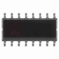
L6574D013TR STMicroelectronics, L6574D013TR Datasheet - Page 3

L6574D013TR
Manufacturer Part Number
L6574D013TR
Description
IC DRIVER BALLAST CFL/TL 16SOIC
Manufacturer
STMicroelectronics
Type
CFL/TL Driverr
Datasheet
1.L6574D013TR.pdf
(10 pages)
Specifications of L6574D013TR
Frequency
60 ~ 120 kHz
Current - Supply
2mA
Current - Output
450mA
Voltage - Supply
10 V ~ 15.6 V
Operating Temperature
-40°C ~ 125°C
Package / Case
16-SOIC (3.9mm Width)
Product
Half-Bridge Drivers
Rise Time
120 ns
Fall Time
80 ns
Supply Voltage (min)
10 V
Supply Current
25 mA
Maximum Operating Temperature
+ 125 C
Mounting Style
SMD/SMT
Bridge Type
Half Bridge
Minimum Operating Temperature
- 40 C
Number Of Drivers
2
Number Of Outputs
2
For Use With
497-8225 - BOARD EVAL BASED ON L6574497-5576 - BOARD EVAL L6574 STD7NS20T4497-3823 - EVAL BOARD FOR HF TL BALLAST
Lead Free Status / RoHS Status
Lead free / RoHS Compliant
Other names
497-4018-2
Available stocks
Company
Part Number
Manufacturer
Quantity
Price
Company:
Part Number:
L6574D013TR
Manufacturer:
ST
Quantity:
2 017
Part Number:
L6574D013TR
Manufacturer:
ST
Quantity:
20 000
PIN DESCRIPTION (continued)
ABSOLUTE MAXIMUM RATINGS
(*) The device has an internal Clamping Zener between GND and the V
a Low Impedance Voltage Source.
Note: ESD immunity for pins 14, 15 and 16 is guaranteed up to 900V (Human Body Model)
V
dV
I
dV
Symbol
EN1
EN1
T
V
N°
10
12
13
14
15
16
11
V
V
V
T
BOOT
9
V
V
V
stg
BOOT
OUT
V
V
OUT
HVG
I
LVG
amb
opd
opo
, V
, I
opc
S
ic
ir
, T
EN2
/dt
EN2
/dt
j
VBOOT
GND
HVG
N.C.
OUT
EN2
LVG
Pin
Supply Current (*)
Low Side Output
High Side Reference
High Side Output
Floating Supply Voltage
V
OUT pin Slew Rate (repetitive)
Forced Input Voltage (pins Ring, Rpre)
Forced Input Voltage (pins Cpre, Cf)
Enable Input Voltage
Enable Input Current
Sense Op Amp Common Mode Range
Sense Op Amp Differential Mode Range
Sense Op Amp Output Voltage (forced)
Storage Temperature
Ambient Temperature
VS
BOOT
pin Slew rate (repetitive)
Enable 2. EN2 input (active high) restarts the start-up procedure (preheating and ignition
sequence). This features is useful if the lamp does not turn-on after the first ignition sequence .
Ground.
Low Side Driver Output. This pin must be connected to the low side power MOSFET gate of the
half bridge. A resistor connected between this pin and the power MOS gate can be used to
reduce the peak current.
Supply Voltage. This pin, connected to the supply filter capacitor, is internally clamped (15.6V
typical).
Non Connected. This pin set a distance between the pins related to the HV and those related to
the LV side.
High Side Driver Floating Reference. This pin must be connected close to the source of the high
side power MOS or IGBT.
High Side Driver Output. This pin must be connected to the high side power MOSFET gate of the
half bridge. A resistor connected between this pin and the power MOS gate can be used to
reduce the peak current.
Bootstrapped Supply Voltage. Between this pin and VS must be connected the bootstrap capac-
itor. A patented integrated circuitry replaces the external bootstrap diode, by means of a high
voltage DMOS, synchronously driven with the low side power MOSFET.
Parameter
Function
CC
pin, it must not be supplied by
-1 to VBOOT -18
-0.3 to Vs +0.3
-1 to VBOOT
-40 to +150
-40 to +125
-1 to 618
-0.3 to 5
-0.3 to 5
-0.3 to 5
-0.3 to 5
Value
4.6
25
50
50
3
5
L6574
Unit
V/ns
V/ns
mA
mA
°C
°C
V
V
V
V
V
V
V
V
V
V
3/10


