TC4420MJA Microchip Technology, TC4420MJA Datasheet - Page 8
TC4420MJA
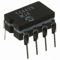
Manufacturer Part Number
TC4420MJA
Description
IC MOSFET DRIVER 6A HS 8CDIP
Manufacturer
Microchip Technology
Type
Microcontrollerr
Specifications of TC4420MJA
Number Of Outputs
1
Package / Case
8-CDIP (0.300", 7.62mm)
Configuration
Low-Side
Input Type
Non-Inverting
Delay Time
55ns
Current - Peak
6A
Number Of Configurations
1
Voltage - Supply
4.5 V ~ 18 V
Operating Temperature
-55°C ~ 125°C
Mounting Type
Through Hole
Rise Time
35 ns
Fall Time
35 ns
Supply Voltage (min)
4.5 V
Supply Current
3 mA
Maximum Operating Temperature
+ 125 C
Mounting Style
Through Hole
Minimum Operating Temperature
- 55 C
Number Of Drivers
1
Lead Free Status / RoHS Status
Lead free / RoHS Compliant
High Side Voltage - Max (bootstrap)
-
Lead Free Status / Rohs Status
Lead free / RoHS Compliant
Other names
TC4420MJAR
TC4420MJAR
TC4420MJAR
Available stocks
Company
Part Number
Manufacturer
Quantity
Price
Company:

Part Number:
TC4420MJA
Manufacturer:
Microchip
Quantity:
5 510
Company:
Part Number:
TC4420MJA
Manufacturer:
ATC
Quantity:
5 510
Company:
Part Number:
TC4420MJA/883C
Manufacturer:
BB
Quantity:
5


TC4420/TC4429
3.0
The descriptions of the pins are listed in Table 3-1.
TABLE 3-1:
3.1
The V
and is rated for 4.5V to 18V with respect to the ground
pins. The V
a local ceramic capacitor. The value of the capacitor
should be chosen based on the capacitive load that is
being driven. A minimum value of 1.0 µF is suggested.
3.2
The MOSFET driver input is a high-impedance,
TTL/CMOS compatible input. The input circuitry of the
TC4420/TC4429 MOSFET driver also has a “speed-
up” capacitor. This helps to decrease the propagation
delay times of the driver. Because of this, input signals
with slow rising or falling edges should not be used, as
this can result in double-pulsing of the MOSFET driver
output.
DS21419C-page 8
8-Pin CERDIP/
PDIP/SOIC
Pin No.
DD
—
—
1
2
3
4
5
6
7
8
PIN DESCRIPTIONS
Supply Input (V
input is the bias supply for the MOSFET driver
Control Input
DD
input should be bypassed to ground with
PIN FUNCTION TABLE
8-Pin DFN
Pin No.
PAD
—
1
2
3
4
5
6
7
8
DD
)
5-Pin TO-220
Pin No.
TAB
—
—
—
—
1
2
4
5
3
OUTPUT
OUTPUT
Symbol
INPUT
GND
GND
V
V
V
NC
NC
DD
DD
DD
3.3
The MOSFET driver output is a low-impedance,
CMOS, push-pull style output capable of driving a
capacitive load with 6.0A peak currents. The MOSFET
driver output is capable of withstanding 1.5A peak
reverse currents of either polarity.
3.4
The ground pins are the return path for the bias current
and the high peak currents that discharge the load
capacitor. The ground pins should be tied into a ground
plane or have very short traces to the bias supply
source return.
3.5
The exposed metal pad of the 6x5 DFN package is not
internally connected to any potential. Therefore, this
pad can be connected to a ground plane or other
copper plane on a printed circuit board (PCB) to aid in
heat removal from the package.
Supply input, 4.5V to 18V
Control input, TTL/CMOS compatible input
No Connection
Ground
Ground
CMOS push-pull output
CMOS push-pull output
Supply input, 4.5V to 18V
Exposed Metal Pad
Metal Tab is at the V
CMOS Push-Pull Output
Ground
Exposed Metal Pad
Description
2004 Microchip Technology Inc.
DD
Potential
Related parts for TC4420MJA
Image
Part Number
Description
Manufacturer
Datasheet
Request
R

Part Number:
Description:
(TC4420 /TC4429) 6A HIGH-SPEED MOSFET DRIVERS
Manufacturer:
Microchip Technology
Datasheet:

Part Number:
Description:
Manufacturer:
Microchip Technology Inc.
Datasheet:
Part Number:
Description:
Manufacturer:
Microchip Technology Inc.
Datasheet:
Part Number:
Description:
Manufacturer:
Microchip Technology Inc.
Datasheet:
Part Number:
Description:
Manufacturer:
Microchip Technology Inc.
Datasheet:
Part Number:
Description:
Manufacturer:
Microchip Technology Inc.
Datasheet:
Part Number:
Description:
Manufacturer:
Microchip Technology Inc.
Datasheet:
Part Number:
Description:
Manufacturer:
Microchip Technology Inc.
Datasheet:
Part Number:
Description:
Manufacturer:
Microchip Technology Inc.
Datasheet: