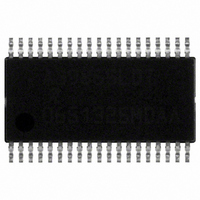
A3985SLDTR-T Allegro Microsystems Inc, A3985SLDTR-T Datasheet - Page 8

A3985SLDTR-T
Manufacturer Part Number
A3985SLDTR-T
Description
IC MOSFET DRVR PROG DUAL 38TSSOP
Manufacturer
Allegro Microsystems Inc
Datasheet
1.A3985SLDTR-T.pdf
(15 pages)
Specifications of A3985SLDTR-T
Configuration
H Bridge
Input Type
Non-Inverting
Delay Time
120ns
Number Of Configurations
2
Number Of Outputs
8
Voltage - Supply
12 V ~ 50 V
Operating Temperature
-20°C ~ 85°C
Mounting Type
Surface Mount
Package / Case
38-TSSOP
Device Type
Full Bridge
Module Configuration
Full Bridge
Peak Output Current
500nA
Output Resistance
19ohm
Input Delay
120ns
Output Delay
120ns
Supply Voltage Range
12V To 50V
Lead Free Status / RoHS Status
Lead free / RoHS Compliant
Current - Peak
-
High Side Voltage - Max (bootstrap)
-
Lead Free Status / RoHS Status
Lead free / RoHS Compliant, Lead free / RoHS Compliant
Other names
620-1180-2
Available stocks
Company
Part Number
Manufacturer
Quantity
Price
Part Number:
A3985SLDTR-T
Manufacturer:
ALLEGRO/雅丽高
Quantity:
20 000
A3985
SDI, SCK, STR, SDO These are the serial port interface
pins. Data is clocked into SDI by a clock signal on SCK. The
data is then latched by a signal on STR. Note, however, that
SCK must be high for one setup time interval, t
STR goes high and SCK must remain high for one hold time
interval, t
Timing Diagram). If required, the serial data out pin, SDO,
can be used to read back the previously-latched serial data or
to form a daisy chain for multiple controllers using a single
STR connection. (For bit assignment details, see the Bit
Assignments table.)
WC This input provides a lockout capability for writing
to the Control register. When set to logic high, no changes
can be made to the Control register through the serial port.
When at logic low, the data on the serial port will update the
Control register (if selected by D0 = 1) while STR is high.
This provides a mechanism to avoid inadvertently changing
the Control register settings by erroneous or corrupt serial
data signals.
Gate Drive
The A3985 is designed to drive external power N-chan-
nel MOSFETs. It supplies the transient currents necessary
to quickly charge and discharge the external FET gate
capacitance in order to reduce dissipation in the external
FET during switching. The charge and discharge rate can
be controlled using an external resistor, RGx, in series with
the connection to the gate of the FET. Cross-conduction is
prevented by the gate drive circuits which introduce a dead
time, t
mentary FET on. t
master clock, depending on the corresponding value set in
the Control register (Word 1: bits D1 and D2). t
up to 1 cycle longer than the programmed value, to allow
synchronization with the master clock.
ENABLE This input simply turns off all of the power MOS-
FETs. Set to logic high to disable outputs. When at logic low,
the internal control enables the outputs as required. Inputs to
the registers and the internal sequencing logic are all active
independent of the ENABLE input state.
C1A, C1B, C2A, and C2B High-side connections for the
bootstrap capacitors, CBOOTx, and positive supply for high-
DEAD
STRH
, between switching one FET off and the comple-
, after STR has gone high (see Serial Data
DEAD
is at least 2, 3, 4, or 6 periods of the
STLG
DEAD
, before
can be
Dual Full-Bridge MOSFET Driver
side gate drivers. The bootstrap capacitors are charged to
approximately V
is low. When the output swings high, the voltage on this ter-
minal rises with the output to provide the boosted gate volt-
age needed for the high-side N-channel power MOSFETs.
The bootstrap capacitor should be ceramic and have a value
of 10 to 20 times the total MOSFET gate capacitance.
GH1A, GH1B, GH2A, and GH2B High-side gate drive
outputs for external N-channel MOSFETs. External series
gate resistors can be used to control the slew rate seen at
the gate, thereby controlling the di/dt and dv/dt at the motor
terminals. GHxx = 1 (high) means that the upper half of the
driver is turned on and will source current to the gate of the
high-side MOSFET in the external motor-driving bridge.
GHxx = 0 (low) means that the lower half of the driver is
turned on and will sink current from the external MOSFET
gate circuit to the respective Sxx pin.
S1A, S1B, S2A, and S2B Directly connected to the
motor, these terminals sense the voltages switched across the
load and define the negative supply for the floating high-side
drivers. The discharge current from the high-side MOSFET
gate capacitance flows through these connections which
should have low impedance traces to the MOSFET bridge.
GL1A, GL1B, GL2A, and GL2B Low-side gate drive
outputs for external N-channel MOSFETs. External series
gate resistors (as close as possible to the MOSFET gate)
can be used to reduce the slew rate seen at the gate, thereby
controlling the di/dt and dv/dt at the motor terminals.
GLxx = 1 (high) means that the upper half of the driver is
turned on and will source current to the gate of the low-side
MOSFET in the external motor-driving bridge. GLxx = 0
(low) means that the lower half of the driver is turned on and
will sink current from the gate of the external MOSFET to
the LSSx pin.
LSS1 and LSS2 Low-side return path for discharge of the
gate capacitors, connected to the common sources of the
low-side external FETs through low-impedance traces.
Internal PWM Current Control
Each full-bridge is independently controlled by a fixed off-
time PWM current control circuit that limits the load current
in the phase to a desired value, I
of source and sink MOSFETs are enabled and current flows
REG
Digitally Programmable
when the associated output Sxx terminal
115 Northeast Cutoff
1.508.853.5000; www.allegromicro.com
Allegro MicroSystems, Inc.
Worcester, Massachusetts 01615-0036 U.S.A.
Trip
. Initially, a diagonal pair
8


