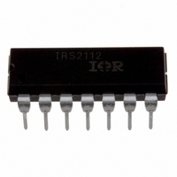
IRS2112PBF International Rectifier, IRS2112PBF Datasheet

IRS2112PBF
Specifications of IRS2112PBF
Available stocks
Related parts for IRS2112PBF
IRS2112PBF Summary of contents
Page 1
Features Floating channel designed for bootstrap operation Fully operational to +600 V Tolerant to negative transient voltage, dV/dt immune Gate drive supply range from Undervoltage lockout for both channels 3.3 V logic compatible Separate logic ...
Page 2
Absolute Maximum Ratings Absolute maximum ratings indicate sustained limits beyond which damage to the device may occur. All voltage param- eters are absolute voltages referenced to COM. The thermal resistance and power dissipation ratings are measured under board mounted and ...
Page 3
Dynamic Electrical Characteristics 1000 pF, T BIAS electrical characteristics are measured using the test circuit shown in Fig. 3. Symbol Definition t Turn-on propagation ...
Page 4
Functional Block Diagram HIN SD LIN Lead Definitions Symbol Description V Logic supply DD HIN Logic input for high-side gate driver output (HO), in phase SD Logic input for shutdown ...
Page 5
Lead Assignments 14 Lead PDIP IRS2112 14 Lead PDIP w/o lead 4 IRS2112-1 www.irf.com IRS2112(-1,-2,S)PbF 16 Lead SOIC (Wide Body) IRS2112S 16 Lead PDIP w/o leads 4 & 5 IRS2112-2 Part Number 5 ...
Page 6
HIN LIN Figure 1. Input/Output Timing Diagram 0 HIN LIN Figure 3. Switching ...
Page 7
M ax. 150 100 Typ -50 - Temperature( C) Figure 7A. Turn-On Propagation Delay Time vs. Temperature 400 M ax. 300 200 Typ. 100 ...
Page 8
M ax. 100 Typ . - Temperature( Figure 9A. Shutdown Delay Time vs. Temperature 400 300 200 T yp. 100 ...
Page 9
Typ Supply Voltage (V ) BIAS Figure 11B. Turn-Off Fall Time vs. Supply Voltage Min. 2.5 5 7.5 10 12.5 V Logic Supply Voltage (V) DD Figure ...
Page 10
M ax 0.2 0 Supply V oltage (V ) BAIS Figure 14B. High Level Output Voltage vs. Supply Voltage ( mA) 1.0 0.8 0.6 0.4 0 ...
Page 11
M ax Floating S upply Voltage ( Figure 17B. V Supply Current vs. Voltage BS 300 250 200 150 100 ...
Page 12
V Logic Supply Voltage (V) DD Figure 20B. Logic “1” Input Current vs Max ...
Page 13
Max. 9 Typ. 8 Min -50 - Temperature (°C) Figure 25. V Undervoltage (-) vs. Temperature CC 500 400 300 200 Typ . 100 M in Supply Voltage ...
Page 14
Frequency (Hz) Figure 28. IRS2112 T vs. Frequency (IRFBC20 GATE CC 150 125 100 1E+2 1E+3 1E+4 ...
Page 15
Frequency (Hz) Figure 34. IRS2112S T vs. Frequency (IRFBC40 GATE CC 0.0 -3.0 Typ. -6.0 -9.0 -12.0 -15 ...
Page 16
Case outline www.irf.com IRS2112(-1,-2,S)PbF 14-Lead PDIP 14-Lead PDIP w/o Lead 4 01-6010 01-3002 03 (MS-001AC) 01-6010 01-3008 02 (MS-001AC) 16 ...
Page 17
Lead PDIP w/o Leads 4 & 5 www.irf.com IRS2112(-1,-2,S)PbF 16-Lead SOIC (wide body) 01-6015 01-3010 02 01 6015 01-3014 03 (MS-013AA) 17 ...
Page 18
Tape & Reel 16-Lead SOIC NTROLLING D IMENSION ...
Page 19
... SPN code) Assembly site code Per SCOP 200-002 ORDER INFORMATION 14-Lead PDIP IRS2112PbF 14-Lead PDIP IRS2112-1PbF 16-Lead PDIP IRS2112-2PbF 16-Lead SOIC IRS2112SPbF This product has been designed and qualified for the industrial level. Qualification standards can be found at www.irf.com Data and specifications subject to change without notice ...


