IR2135JTRPBF International Rectifier, IR2135JTRPBF Datasheet - Page 3
IR2135JTRPBF
Manufacturer Part Number
IR2135JTRPBF
Description
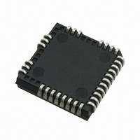
IC DRIVER 3PHASE 44-PLCC
Manufacturer
International Rectifier
Datasheet
1.IR2135STRPBF.pdf
(27 pages)
Specifications of IR2135JTRPBF
Configuration
3 Phase Bridge
Input Type
Inverting
Delay Time
750ns
Current - Peak
200mA
Number Of Configurations
1
Number Of Outputs
3
High Side Voltage - Max (bootstrap)
600V
Voltage - Supply
10 V ~ 20 V
Mounting Type
Surface Mount
Package / Case
44-PLCC (32 Leads)
Device Type
MOSFET
Peak Output Current
420mA
Input Delay
750ns
Output Delay
700ns
Supply Voltage Range
10V To 20V
Driver Case Style
LCC
No. Of Pins
44
Leaded Process Compatible
Yes
Rohs Compliant
Yes
Lead Free Status / RoHS Status
Lead free / RoHS Compliant
Operating Temperature
-
Available stocks
Company
Part Number
Manufacturer
Quantity
Price
Company:

Part Number:
IR2135JTRPBF
Manufacturer:
International Rectifier
Quantity:
10 000


Dynamic Electrical Characteristics
V
NOTE: For high side PWM, HIN pulse width must be
www.irf.com
Static Electrical Characteristics
V
are referenced to V
referenced to COM and V
V
V
V
V
V
V
V
V
V
V
I
I
I
I
I
I
I
I
I
Symbol
Symbol
QCC
BIAS (
LK
QBS
IN +
IN -
SD +
SD -
ITRIP +
ITRIP -
BIAS
SD,TH -
OH
OL
IH
IL
FCLR,IH
FCLR,IL
SD,TH +
IT,TH +
IT,TH -
t on
t off
t r
t f
t sd
t itrip
t bl
t flt
t fil,in
t fltclr
DT
SR+
SR-
(V
V
CC ,
CC ,
V
V
Logic “0” Input Voltage (OUT = LO)
Logic “1” Input Voltage (OUT = HI)
Logic “0” Fault Clear Input Voltage
Logic “1” Fault Clear Input Voltage
SD Input Positive Going Threshold
SD Input Negative Going Threshold
I
I
High Level Output Voltage, V BIAS - V O
Low Level Output Voltage, V O
Offset Supply Leakage Current (IR2133/IR2135)
Quiescent V BS Supply Current
Quiescent V CC Supply Current
Logic “1” Input Bias Current (OUT = HI)
Logic “0” Input Bias Current (OUT = LO)
“High” Shutdown Bias Current
“Low” Shutdown Bias Current
“High” I
“Low” I
Definition
Definition
Turn-on propagation delay
Turn-off propagation delay
Turn-on rise time
Turn-off fall time
SD to output shutdown propagation delay
ITRIP to output shutdown propagation delay
ITRIP blanking time
ITRIP to FAULT propagation delay
Input filter time (HIN, LIN and SD)
FLT-CLR to FAULT clear time
Deadtime, LS turn-off to HS turn-on &
HS turn-off to LS turn-on
Amplifier slew rate (positive)
Amplifier slew rate (negative)
ITRIP
ITRIP
BS1,2,3 )
BS1,2,3
Input Negative Going Threshold
Input Positive Going Threshold
ITRIP
ITRIP
SS
) = 15V unless otherwise specified and T
= 15V, V
and are applicable to all six channels (H
Bias Current
Bias Current
S1,2,3
S1,2,3
and are applicable to the respective output leads: H
=
V
SS
(IR2233/IR2235)
,
IR2133/IR2135/IR2233
T
sec
A
= 25
o
C
and
C
L
A
Min.
Min. Typ. Max. Units Test Conditions
500
450
500
600
400
600
100
—
—
2.2
—
2.2
—
1.6
1.4
470
360
—
—
—
—
—
—
—
—
—
—
—
—
—
—
= 1000
5
2
= 25
S1,2,3
o
Typ. Max. Units
C. All static parameters other than IO and VO
400
310
850
250
—
—
—
—
1.9
1.7
570
460
—
—
—
—
200
100
—
750
700
750
850
650
50
30
30
p
90
40
10
4
—
2.5
& L
F unless otherwise specified.
S1,2,3
1000
1000
1100
1100
950
150
900
400
—
0.8
—
0.8
2.2
2.0
670
560
100
100
100
350
250
100
100
100
100
70
—
—
—
—
50
50
8
). The VO and IO parameters are
/
V/µs
O1,2,3
ns
IR2235(J
mV
µA
mA
µA
nA
µA
nA
V
or L
V
ITRIP = 1V
V
V
V
V
V
V
V
V
V
V
V
V
SD = 5V
SD = 0V
I
I
IN
IN
IN
IN
IN
ITRIP
ITRIP
IN
IN
B1,2,3
B1,2,3
IN
IN
IN
IN
V
,V
,V
,V
O1,2,3.
V
= 0 & 5V
= 0 & 5V
Test Conditions
S1,2,3
= 0V, I O = 0A
= 5V, I O = 0A
= 0V or 5V
= 0V or 5V
= 0V
= 5V
IN
ITRIP
ITRIP
ITRIP
V
,V
= 5V
= 0V
=V
=V
IN
or 1200V
SD
= 0 & 5V
&
= 0 to 600V
S1,2,3
S1,2,3
= 0 & 5V
= 0 & 5V
= 0 & 5V
= 0 & 5V
S
) & (PbF)
= 600V
= 1200V
3
Related parts for IR2135JTRPBF
Image
Part Number
Description
Manufacturer
Datasheet
Request
R

Part Number:
Description:
IC DRIVER BRIDGE 3-PHASE 44-PLCC
Manufacturer:
International Rectifier
Datasheet:

Part Number:
Description:
SCHOTTKY RECTIFIER
Manufacturer:
International Rectifier Corp.
Datasheet:
Part Number:
Description:
SCHOTTKY RECTIFIER
Manufacturer:
International Rectifier Corp.
Datasheet:
Part Number:
Description:
SCHOTTKY RECTIFIER
Manufacturer:
International Rectifier Corp.
Datasheet:
Part Number:
Description:
SCHOTTKY RECTIFIER
Manufacturer:
International Rectifier Corp.
Datasheet:
Part Number:
Description:
SCHOTTKY RECTIFIER
Manufacturer:
International Rectifier Corp.
Datasheet:
Part Number:
Description:
SCHOTTKY RECTIFIER
Manufacturer:
International Rectifier Corp.
Datasheet:
Part Number:
Description:
SCHOTTKY RECTIFIER
Manufacturer:
International Rectifier Corp.
Datasheet:
Part Number:
Description:
SCHOTTKY RECTIFIER
Manufacturer:
International Rectifier Corp.
Datasheet:
Part Number:
Description:
SCHOTTKY RECTIFIER
Manufacturer:
International Rectifier Corp.
Datasheet:
Part Number:
Description:
SCHOTTKY RECTIFIER
Manufacturer:
International Rectifier Corp.
Datasheet:
Part Number:
Description:
SCHOTTKY RECTIFIER
Manufacturer:
International Rectifier Corp.
Datasheet:
Part Number:
Description:
SCHOTTKY RECTIFIER
Manufacturer:
International Rectifier Corp.
Datasheet:
Part Number:
Description:
SCHOTTKY RECTIFIER
Manufacturer:
International Rectifier Corp.
Datasheet:
Part Number:
Description:
SCHOTTKY RECTIFIER
Manufacturer:
International Rectifier Corp.
Datasheet: