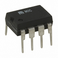
MIC4425BN Micrel Inc, MIC4425BN Datasheet

MIC4425BN
Specifications of MIC4425BN
Available stocks
Related parts for MIC4425BN
MIC4425BN Summary of contents
Page 1
MIC4423/4424/4425 General Description The MIC4423/4424/4425 family are highly reliable BiCMOS/ DMOS buffer/driver/MOSFET drivers. They are higher out- put current versions of the MIC4426/4427/4428, which are improved versions of the MIC426/427/428. All three families are pin-compatible. The MIC4423/4424/4425 drivers are ca- ...
Page 2
... MIC4423YWM MIC4423BM MIC4423YM MIC4423CN MIC4423ZN MIC4423BN MIC4423YN MIC4424CWM MIC4424ZWM MIC4424BWM MIC4424YWM MIC4424BM MIC4424YM MIC4424CN MIC4424ZN MIC4424BN MIC4424YN MIC4425CWM MIC4425ZWM MIC4425BWM MIC4425YWM MIC4425BM MIC4425YM MIC4425CN Contact Factory MIC4425BN MIC4425YN Pin Configuration INA 2 7 OUTA GND INB 8-pin DIP (N) 8-pin SOIC ( INA 2 ...
Page 3
MIC4423/4424/4425 Absolute Maximum Ratings Supply Voltage ........................................................... +22V Input Voltage .................................. V Junction Temperature ................................................150°C Storage Temperature Range ......................–65°C to 150°C Lead Temperature (10 sec.) ......................................300°C ESD Susceptability, Note 3 ..................................... 1000V MIC4423/4424/4425 Electrical Characteristics 4.5V ≤ V ≤ 18V; ...
Page 4
MIC4423/4424/4425 Test Circuit V = 18V S 0.1µF INA A 1800pF MIC4423 B INB 1800pF 5V 90% INPUT 10 90 TPU T 10% 0V Figure 1a. Inverting Driver ...
Page 5
MIC4423/4424/4425 Typical Characteristic Curves Rise Time vs. Supply Voltage 100 4700pF 80 1800pF 3300pF 60 1000pF 2200pF 40 20 470pF (V) SUPPLY Fall Time vs. Capacitive Load 100 80 5V ...
Page 6
MIC4423/4424/4425 Delay Time vs. Supply Voltage 2200 pF LOAD (V) SUPPLY Quiescent Current vs. Temperature 1 ...
Page 7
MIC4423/4424/4425 Application Information Although the MIC4423/24/25 drivers have been specifically constructed to operate reliably under any practical circum- stances, there are nonetheless details of usage which will provide better operation of the device. Supply Bypassing Charging and discharging large capacitive ...
Page 8
MIC4423/4424/4425 ground pin of the driver directly to the ground terminal of the load. Do not use a twisted pair where the second wire in the pair is the output of the other driver, as this will not provide a ...
Page 9
MIC4423/4424/4425 frequency, power supply voltage, and load all affect power dissipation. Given the power dissipation in the device, and the thermal resistance of the package, junction operating temperature for any ambient is easy to calculate. For example, the ther- mal ...
Page 10
MIC4423/4424/4425 Then quiescent power loss – [(0.5 x 0.0035) + (0.5 x 0.0003)] = 0.0228W Total power dissipation, then, is ...
Page 11
MIC4423/4424/4425 NOTE: THE VALUES ON THIS GRAPH REPRESENT THE LOSS SEEN BY BOTH DRIVERS IN A PACKAGE DURING ONE COMPLETE CYCLE. FOR A SINGLE DRIVER DIVIDE THE STATED VALUES BY 2. FOR A SINGLE TRANSITION OF A SINGLE DRIVER, DIVIDE ...
Page 12
MIC4423/4424/4425 Package Information 0.018 (0.57) MIC4423/4424/4425 PIN 1 DIMENSIONS: INCH (MM) 0.380 (9.65) 0.370 (9.40) 0.135 (3.43) 0.125 (3.18) 0.380 (9.65) 0.130 (3.30) 0.320 (8.13) 0.100 (2.54) 0.0375 (0.952) 8-Pin Plastic DIP (N) 8-Pin SOIC (M) 12 Micrel, Inc. 0.255 ...
Page 13
... MICREL INC. 2180 FORTUNE DRIVE SAN JOSE, CA 95131 USA + 1 (408) 944-0800 TEL This information furnished by Micrel in this data sheet is believed to be accurate and reliable. However no responsibility is assumed by Micrel for its use. Micrel reserves the right to change circuitry and specifications at any time without notification to the customer. ...


