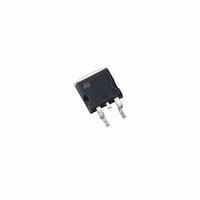
VNB20N07 STMicroelectronics, VNB20N07 Datasheet

VNB20N07
Specifications of VNB20N07
Available stocks
Related parts for VNB20N07
VNB20N07 Summary of contents
Page 1
... PIN ESD PROTECTION DIRECT ACCESS TO THE GATE OF THE POWER MOSFET (ANALOG DRIVING) COMPATIBLE WITH STANDARD POWER MOSFET DESCRIPTION The VNP20N07FI, VNB20N07 and VNV20N07 are monolithic devices STMicroelectronics VlPower M0 Technology, intended for replacement of standard power MOSFETS KHz applications. Built-in thermal shut-down, linear current limitation and ...
Page 2
... VNP20N07FI-VNB20N07-VNV20N07 ABSOLUTE MAXIMUM RATING Symbol Parameter V Drain-source Voltage ( Input Voltage in I Drain Current D I Reverse DC Output Current R V Electrostatic Discharge (C= 100 pF, R=1 esd P Total Dissipation at T tot T Operating Junction Temperature j T Case Operating Temperature c T Storage Temperature stg THERMAL DATA R Thermal Resistance Junction-case ...
Page 3
... Drain Current Limit lim Step Response dlim Current Limit Overtemperature jsh Shutdown Overtemperature Reset jrs Fault Sink Current Single Pulse as Avalanche Energy ( ) Pulsed: Pulse duration = 300 s, duty cycle 1 Parameters guaranteed by design/characterization VNP20N07FI-VNB20N07-VNV20N07 Test Conditions gen gen (see figure 1000 gen gen (see figure ...
Page 4
... VNP20N07FI-VNB20N07-VNV20N07 PROTECTION FEATURES During normal operation, the Input pin is electrically connected to the gate of the internal power MOSFET. The device then behaves like a standard power MOSFET and can be used as a switch from KHz. The only difference from the user’s standpoint is that a small DC ...
Page 5
... Thermal Impedance For ISOWATT220 Derating Curve Transconductance VNP20N07FI-VNB20N07-VNV20N07 Thermal Impedance For D2PAK / PowerSO-10 Output Characteristics Static Drain-Source On Resistance vs Input Voltage 5/13 ...
Page 6
... VNP20N07FI-VNB20N07-VNV20N07 Static Drain-Source On Resistance Input Charge vs Input Voltage Normalized Input Threshold Voltage vs Temperature 6/13 Static Drain-Source On Resistance Capacitance Variations Normalized On Resistance vs Temperature ...
Page 7
... Normalized On Resistance vs Temperature Turn-on Current Slope Turn-off Drain-Source Voltage Slope VNP20N07FI-VNB20N07-VNV20N07 Turn-on Current Slope Turn-off Drain-Source Voltage Slope Switching Time Resistive Load 7/13 ...
Page 8
... VNP20N07FI-VNB20N07-VNV20N07 Switching Time Resistive Load Current Limit vs Junction Temperature Source Drain Diode Forward Characteristics 8/13 Switching Time Resistive Load Step Response Current Limit ...
Page 9
... Fig. 1: Unclamped Inductive Load Test Circuits Fig. 3: Switching Times Test Circuits For Resistive Load Fig. 5: Test Circuit For Inductive Load Switching And Diode Recovery Times VNP20N07FI-VNB20N07-VNV20N07 Fig. 2: Unclamped Inductive Waveforms Fig. 4: Input Charge Test Circuit Fig. 6: Waveforms 9/13 ...
Page 10
... VNP20N07FI-VNB20N07-VNV20N07 ISOWATT220 MECHANICAL DATA DIM. MIN. A 4.4 B 2.5 D 2.5 E 0.4 F 0.75 F1 1.15 F2 1.15 G 4. 28.6 L4 9 Ø 3 ¯ 10/13 mm TYP. MAX. MIN. 4.6 0.173 2.7 0.098 2.75 0.098 0.7 0.015 1 0.030 1.7 0.045 1.7 0.045 5.2 0.195 2.7 0.094 10 ...
Page 11
... TO-263 (D2PAK) MECHANICAL DATA DIM. MIN. A 4.3 A1 2.49 B 0.7 B2 1.25 C 0.45 C2 1. 1. VNP20N07FI-VNB20N07-VNV20N07 mm TYP. MAX. MIN. 4.6 0.169 2.69 0.098 0.93 0.027 1.4 0.049 0.6 0.017 1.36 0.047 9.35 0.352 10.28 0.393 5.28 0.192 15.85 0.590 1.4 0.050 1.75 0.055 inch TYP ...
Page 12
... VNP20N07FI-VNB20N07-VNV20N07 PowerSO-10 MECHANICAL DATA DIM. MIN. A 3.35 A1 0.00 B 0.40 c 0.35 D 9.40 D1 7.40 E 9.30 E1 7.20 E2 7.20 E3 6. 1.25 H 13 12/13 mm TYP. MAX. 3.65 0.10 0.60 0.55 9.60 7.60 9.50 7.40 7.60 6.35 6.10 1.27 1.35 14.40 0.50 1. SEATING PLANE DETAIL " ...
Page 13
... STMicroelectronics – Printed in Italy – All Rights Reserved Australia - Brazil - Canada - China - France - Germany - Italy - Japan - Korea - Malaysia - Malta - Mexico - Morocco - The Netherlands - Singapore - Spain - Sweden - Switzerland - Taiwan - Thailand - United Kingdom - U.S.A. VNP20N07FI-VNB20N07-VNV20N07 The ST logo is a trademark of STMicroelectronics STMicroelectronics GROUP OF COMPANIES ...


