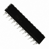
L6227N STMicroelectronics, L6227N Datasheet - Page 9

L6227N
Manufacturer Part Number
L6227N
Description
IC DRIVER FULL BRIDGE DUAL 24DIP
Manufacturer
STMicroelectronics
Type
H Bridger
Datasheet
1.L6227DTR.pdf
(22 pages)
Specifications of L6227N
Input Type
Non-Inverting
Number Of Outputs
4
On-state Resistance
730 mOhm
Current - Output / Channel
1.4A
Current - Peak Output
2.8A
Voltage - Supply
8 V ~ 52 V
Operating Temperature
-25°C ~ 125°C
Mounting Type
Through Hole
Package / Case
PowerSSO-24
Operating Supply Voltage
8 V to 52 V
Supply Current
1.4 A
Mounting Style
Through Hole
For Use With
497-6817 - EVAL BOARD FOR L6227Q
Lead Free Status / RoHS Status
Lead free / RoHS Compliant
Other names
497-3648
Available stocks
Company
Part Number
Manufacturer
Quantity
Price
Company:
Part Number:
L6227N
Manufacturer:
STMicroelectronics
Quantity:
750
TRUTH TABLE
X
High Z
GND (Vs)
(*) Valid only in case of load connected between OUT1 and OUT2
PWM CURRENT CONTROL
The L6227 includes a constant off time PWM current controller for each of the two bridges. The current control
circuit senses the bridge current by sensing the voltage drop across an external sense resistor connected be-
tween the source of the two lower power MOS transistors and ground, as shown in Figure 7. As the current in
the load builds up the voltage across the sense resistor increases proportionally. When the voltage drop across
the sense resistor becomes greater than the voltage at the reference input (VREF
parator triggers the monostable switching the low-side MOS off. The low-side MOS remain off for the time set
by the monostable and the motor current recirculates in the upper path. When the monostable times out the
bridge will again turn on. Since the internal dead time, used to prevent cross conduction in the bridge, delays
the turn on of the power MOS, the effective off time is the sum of the monostable time plus the dead time.
Figure 7. PWM Current Controller Simplified Schematic
Figure 8 shows the typical operating waveforms of the output current, the voltage drop across the sensing re-
sistor, the RC pin voltage and the status of the bridge. Immediately after the low-side Power MOS turns on, a
high peak current flows through the sensing resistor due to the reverse recovery of the freewheeling diodes. The
L6227 provides a 1 s Blanking Time t
prematurely re-trigger the monostable.
EN
H
H
H
H
L
5V
C
5mA
= GND during Ton, Vs during Toff
= Don't care
= High Impedance Output
(0)
INPUTS
TO GATE LOGIC
IN1
H
H
RC A(or B)
R
X
L
L
(1)
2.5V
Q
+
-
IN2
S
R
H
H
X
L
L
MONOSTABLE
BLANKING TIME
MONOSTABLE
RESET
BLANK
GND (Vs)
High Z
OUT1
GND
Vs
Vs
COMPARATOR
that inhibits the comparator output so that this current spike cannot
OUTPUT
BLANKER
1 s
COMPARATOR
OUTPUTS
SENSE
DEAD TIME
DRIVERS
+
-
GND (Vs)
+
VREF A(or B)
GATE DRIVERS
High Z
OUT2
GND
FROM THE
LOW-SIDE
Vs
Vs
2H
R SENSE
2L
DEAD TIME
VS
DRIVERS
Disable
Brake Mode (Lower Path)
Forward
Reverse
Brake Mode (Upper Path)
A
+
(or B)
SENSE A(or B)
A
1H
1L
or VREF
Description (*)
OUT2 A(or B)
OUT1 A(or B)
D02IN1352
I OUT
B
) the sense com-
LOAD
(or
B
)
A
L6227
9/22


