BTS555 E3146 Infineon Technologies, BTS555 E3146 Datasheet
BTS555 E3146
Specifications of BTS555 E3146
BTS555E3146
BTS555E3146IN
BTS555E3146NK
SP000011265
SP000842742


Related parts for BTS555 E3146


BTS555 E3146 Summary of contents
Page 1
... Due to the different lead frame geometry Ron @25°C is 0.3 m higher in staggered than in straight version, and accordingly for other temperatures With additional external diode. 3) Additional external diode required for energized inductive loads (see page 9). Infineon Technologies AG Product Summary Overvoltage protection Output clamp Operating voltage On-state resistance Load current (ISO) ...
Page 2
... V is setup without the DUT connected to the generator per ISO 7637-1 and DIN 40839. Load dump Infineon Technologies AG Function Output to the load. The pins 1 and 5 must be shorted with each other especially in high current applications! Input, activates the power switch in case of short to ground Positive power supply voltage, the tab is electrically connected to this pin ...
Page 3
... Decrease of V below 10 V causes slowly a dynamic increase long as V > bIN bIN(u) max ON 10) not subject to production test, specified by design 11 about 105°C under these conditions See timing diagram on page 14. 12 Infineon Technologies AG R chip - case : ° 150 ° 120 150 ° ...
Page 4
... For the voltage range 0..34 V the device is fully protected against overtemperature and short circuit see diagram on page 7. When bIN (typ.) the charge pump is not active and V 15) See also V in circuit diagram on page 8. ON(CL) Infineon Technologies ° 150 ° (Pins 1,5 to Tab > ...
Page 5
... Note that under off-conditions (I is not activated. This results in raised power dissipation due to the higher voltage drop across the intrinsic drain-source diode. The temperature protection is not active during reverse current operation! Increasing reverse battery voltage capability is simply possible as described on page 9. Infineon Technologies AG Symbol =-40° ...
Page 6
... ON I saturation, see . IS,lim ) not subject to production test, specified by design recommend the resistance between IN and GND to be less than 0 500 for turn-off. Consider that when the device is switched off (I reaches almost Infineon Technologies 120 A,T =-40° =25° =150° A,T =-40°C: ...
Page 7
... Terms 3 V bIN PROFET bIS Two or more devices can easily be connected in parallel to increase load current capability. ) Low ohmic short may reduce the output current Power Transistor "OFF", potential defined by external impedance. 24 Infineon Technologies AG Output Current Sense level nominal H I IS, lim <nominal ...
Page 8
... Note: For large values of R the voltage V IS almost V . See also overvoltage protection you don't use the current sense output in your application, you can leave it open. Infineon Technologies AG Short circuit detection Fault Condition (80 ...300 µs Inductive and overvoltage output clamp = 0) the voltage IN ...
Page 9
... Provide a current path with load current capability by using a diode, a Z-diode varistor < =0). For higher clamp voltages Zb IN currents at IN and IS have to be limited to 250 mA. Version PROFET IS Infineon Technologies AG Version OUT Power Transistor Note that there is no reverse battery protection when Power GND ...
Page 10
... with an approximate solution for R L · OUT(CL · L Infineon Technologies AG Maximum allowable load inductance for a single switch off j,start = 150° 1000000 - I L OUT 100000 V + OUT 10000 R IS 1000 = 0 [µH] Externally adjustable current limit the device is conducting, the sense current can be ...
Page 11
... Overvoltage shutdown Output negative voltage transient limit ON(CL -15 V typ OUT ) Latch except when OUT 0 V only if forced externally). So the device remains latched unless V between turn on and t . d(SC) ) Can be "switched off" by using a diode D 26 Infineon Technologies AG BTS 6510 550P 650P 26 < V after shutdown ...
Page 12
... ILIS ilis 65000 60000 55000 50000 45000 40000 max 35000 typ 30000 25000 min 20000 0 50 100 Infineon Technologies AG Current sense ratio f(I ILIS k ilis 65000 60000 55000 50000 45000 40000 min 35000 30000 25000 20000 150 I [A] L Current sense ratio: ...
Page 13
... ON(SC) switched off by internal short circuit detection. Typ. on-state resistance [mOhm 150° 85°C 25°C 2 -40° Infineon Technologies AG Typ. input current bIN I [mA] IN 1.6 1.4 1.2 only for t < t d(SC) 1.0 0.8 25°C 0.6 0.4 150° static dynamic 15 20 ...
Page 14
... The sense signal is not valid during a settling time after turn-on/off and after change of load current. Figure 2a: Switching motors and lamps OUT Sense current saturation can occur at very high inrush currents (see I on page 6). IS,lim Infineon Technologies AG Figure 2b: Switching an inductive load dV/dtoff V OUT t off t slc(IS ...
Page 15
... Figure 4a: Overtemperature, Reset if (I =low) and (T < OUT T J Figure 6a: Undervoltage restart of charge pump, overvoltage clamp V OUT V IN dynamic, short 6 Undervoltage not below V bIN( bIN(u) bIN(ucp) Infineon Technologies ON(CL ON(CL) 15 Data Sheet BTS555 2008-June-24 ...
Page 16
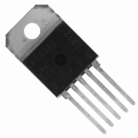
... Package and Ordering Code All dimensions in mm TO-218AB/5 Option E3146 BTS555 E3146 15 ±0.2 14.8 10.8 ±0.2 +0. 0...0.1 +0.2 1.1 0.5 2.54 0. 2.54 = 10.16 1) Punch direction, burr max. 0.04 General tolerances ± 0.1 TO-218AB/5-1 BTS555 15 ±0.2 14.8 10.8 ±0.2 +0. 0...0.1 +0 ...