IPS6031RPBF International Rectifier, IPS6031RPBF Datasheet - Page 3
IPS6031RPBF
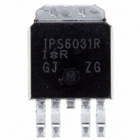
Manufacturer Part Number
IPS6031RPBF
Description
INTELLIGENT POWER SW 1CH DPAK-5
Manufacturer
International Rectifier
Type
High Sider
Datasheet
1.IPS6031PBF.pdf
(14 pages)
Specifications of IPS6031RPBF
Input Type
Non-Inverting
Number Of Outputs
1
On-state Resistance
46 mOhm
Current - Output / Channel
2.8A
Current - Peak Output
16A
Voltage - Supply
6 V ~ 28 V
Operating Temperature
-40°C ~ 150°C
Mounting Type
Surface Mount
Package / Case
DPak, TO-252 (4 leads + tab)
Switch Type
High Side
Power Switch Family
IPS6031
Input Voltage
-0.3 to 5.5V
Power Switch On Resistance
55mOhm
Output Current
2.8A
Mounting
Surface Mount
Supply Current
2.2mA
Package Type
DPAK
Operating Temperature (min)
-40C
Operating Temperature (max)
150C
Operating Temperature Classification
Automotive
Pin Count
4 +Tab
Power Dissipation
2.5W
Current, Drain
8.9 A
Current, Input
100 μA
Current, Leakage, Offset
10 μA
Current, Supply
5 A
Polarization
N-Channel
Resistance, Drain To Source On
60 Milliohms
Temperature, Operating, Maximum
+150 °C
Temperature, Operating, Minimum
–40 °C
Thermal Resistance, Junction To Ambient
50 °C/W
Time, Turn-off Delay
25 μs
Time, Turn-on Delay
45 μs
Voltage, Input
5.5 V
Voltage, Input, High Level
5.5 V
Voltage, Input, Low Level
0.9 V
Voltage, Supply
36 V
Power Load Switch Type
High Side
Current Limit
16A
On State Resistance
0.046ohm
Thermal Protection
Yes
On / Enable Input Polarity
Active High
Power Dissipation Pd
2.5W
Rohs Compliant
Yes
Lead Free Status / RoHS Status
Lead free / RoHS Compliant
Available stocks
Company
Part Number
Manufacturer
Quantity
Price


Static Electrical Characteristics
Tj=25°C, Vcc=14V (unless otherwise specified)
S
Vcc=14V, Resis
www.irf.com
Symbol
Rds(on)
Vcc op.
V clamp 1
V clamp 2
Icc Off
Icc On
Vih
Vil
In hyst.
Iin On
Idg
Vdg
Symbol
Tdon
Tr1
Tr2
dV/dt (On)
EOn
Tdoff
Tf
dV/dt (Off)
EOff
witc
hing lectrical Characteris
Parameter
ON state resistance Tj=25°C
ON state resistance Tj=150°C
O
ON state resistance during reverse battery
Operating voltage range
V
V
S
S
I
I nput low threshold voltage
Input hysteresis
Input current when device is On
Dg leakage current
L
tive load=6Ω, Vin=5V, Tj=25°C
nput high threshold voltage
ow level DG voltage
Parameter
Turn-on delay time
Rise time to Vout=Vcc-5V
Rise time to Vout=0.9 x Vcc
Turn On dV/dt
Turn On energy
T
F
T
T
cc to Out clamp voltage 1
cc to Out clamp voltage 2
upply current when O
upply current when On
E
N state resistance Tj=25°C, Vcc=6V
urn-off delay ti
all time to Vout=0.1 x Vcc
urn Off dV/dt
urn Off energy
me
ff
tics
Min.
Min.
⎯
⎯
⎯
⎯
⎯
⎯
⎯
⎯
⎯
1.5
0.2
37
⎯
⎯
⎯
⎯
⎯
⎯
⎯
⎯
⎯
⎯
⎯
6
Typ.
150
1.5
Typ.
20
65
0.25
8
5
8
9
3
2.2
2.5
0.5
0.1
46
83
55
60
39
40
45
⎯
4
2
Max.
2.5
25
20
35
45
30
10
Max.
⎯
⎯
100
100
2.9
0.4
60
72
80
28
42
10
⎯
⎯
9
5
1
IPS6031(
Units
V/µs
V/µs
Units
µs
µJ
µs
µJ
mΩ
mA
µA
µA
V
V
V
T
see Fig. 3
est
Test Conditions
Vin= V, Iout= A
Vin=5V, Iout=5
Vin=5V, Iout=2
Vcc
Iou
Iou
Vin
Vin
Vin
Vd
Id
g=1.6m
g=5V
t=30
t=4A
=0V
=5V
=5V
Conditions
-Gn
5
S
, Vou
d=14
mA
)(
(see
A
R
V
t=0V
Fig. 1)
5
)PbF
A
.5A
3
Related parts for IPS6031RPBF
Image
Part Number
Description
Manufacturer
Datasheet
Request
R

Part Number:
Description:
SCHOTTKY RECTIFIER
Manufacturer:
International Rectifier Corp.
Datasheet:
Part Number:
Description:
SCHOTTKY RECTIFIER
Manufacturer:
International Rectifier Corp.
Datasheet:
Part Number:
Description:
SCHOTTKY RECTIFIER
Manufacturer:
International Rectifier Corp.
Datasheet:
Part Number:
Description:
SCHOTTKY RECTIFIER
Manufacturer:
International Rectifier Corp.
Datasheet:
Part Number:
Description:
SCHOTTKY RECTIFIER
Manufacturer:
International Rectifier Corp.
Datasheet:
Part Number:
Description:
SCHOTTKY RECTIFIER
Manufacturer:
International Rectifier Corp.
Datasheet:
Part Number:
Description:
SCHOTTKY RECTIFIER
Manufacturer:
International Rectifier Corp.
Datasheet:
Part Number:
Description:
SCHOTTKY RECTIFIER
Manufacturer:
International Rectifier Corp.
Datasheet:
Part Number:
Description:
SCHOTTKY RECTIFIER
Manufacturer:
International Rectifier Corp.
Datasheet:
Part Number:
Description:
SCHOTTKY RECTIFIER
Manufacturer:
International Rectifier Corp.
Datasheet:
Part Number:
Description:
SCHOTTKY RECTIFIER
Manufacturer:
International Rectifier Corp.
Datasheet:
Part Number:
Description:
SCHOTTKY RECTIFIER
Manufacturer:
International Rectifier Corp.
Datasheet:
Part Number:
Description:
SCHOTTKY RECTIFIER
Manufacturer:
International Rectifier Corp.
Datasheet:
Part Number:
Description:
SCHOTTKY RECTIFIER
Manufacturer:
International Rectifier Corp.
Datasheet:
Part Number:
Description:
SCHOTTKY RECTIFIER
Manufacturer:
International Rectifier Corp.
Datasheet: