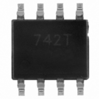
BSP752T Infineon Technologies, BSP752T Datasheet

BSP752T
Specifications of BSP752T
BSP752TNT
BSP752TT
BSP752TT
BSP752TTR
BSP752TXT
SP000012797
SP000278359
Available stocks
Related parts for BSP752T
BSP752T Summary of contents
Page 1
Smart Power High-Side-Switch Features Overload protection Current limitation Short circuit protection Thermal shutdown with restart Overvoltage protection (including load dump) Fast demagnetization of inductive loads Reverse battery protection with external resistor CMOS compatible input Loss of GND and loss of ...
Page 2
Block Diagram Voltage Overvoltage source protection V Logic Charge pump Level shifter Rectifier IN Logic ESD Pin Symbol GND OUT Vbb 5 Vbb 6 Vbb 7 Vbb 8 Pin configuration Top view 1 8 ...
Page 3
Maximum Ratings 25°C, unless otherwise specified j Parameter Supply voltage Supply voltage for full short circuit protection Continuous input voltage Load current (Short - circuit current, see page 5) Current through input pin (DC) Operating temperature Storage ...
Page 4
Electrical Characteristics Parameter and Conditions -40...+150° 12..42V Load Switching Capabilities and Characteristics On-state resistance = 25 ° 9... 150 °C T ...
Page 5
Electrical Characteristics Parameter and Conditions -40...+150° 12..42V Protection Functions Initial peak short circuit current limit (pin -40 ° ...
Page 6
Electrical Characteristics Parameter and Conditions -40...+150° 12..42V Input Input turn-on threshold voltage Input turn-off threshold voltage Input threshold hysteresis Off state input current state input current V ...
Page 7
Terms PROFET V IN GND V I GND bb R GND Input circuit (ESD protection ESD GND The use of ESD zener diodes as voltage clamp ...
Page 8
GND disconnect PROFET GND GND GND disconnect with GND pull OUT PROFET GND GND disconnect with charged inductive load high OUT ...
Page 9
Typ. transient thermal impedance 6cm heatsink area thJA p Parameter: D D=0.5 K/W D=0.2 D=0 D=0.05 D=0. D=0.01 D ...
Page 10
Typ. turn on time 160 µs 120 100 -40 - Typ. slew rate on dV/ ...
Page 11
Typ. standby current 42V ; V bb(off µ -40 - Typ. initial peak short circuit current limit I = f(V ) L(SCp) ...
Page 12
Typ. input current 13,5V; V IN(on/off 0,7V low high 12 µ -40 - Typ. input threshold voltage ...
Page 13
Maximum allowable load inductance for a single switch off =150° jstart L 2000 mH 1600 1400 1200 1000 800 600 42V 400 13,5V 200 0 0 0.25 0.5 0.75 Maximum allowable inductive ...
Page 14
Timing diagrams Figure 1a: Vbb turn on OUT Figure 2a: Switching a resistive load, turn-on/off time and slew rate definition ...
Page 15
Figure 3a: Turn on into short circuit, shut down by overtemperature, restart by cooling L(SCp) I L(SCr off(SC) Heating up of the chip may require several milliseconds, depending on external conditions. Figure 4: ...
Page 16
... Infineon Technologies Office. Infineon Technologies Components may only be used in life-support devices or systems with the express written approval of Infineon Technologies failure of such components can reasonably be expected to cause the failure of that life-support device or system affect the safety or effectiveness of that device or system ...


