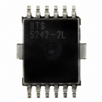
BTS5242-2L Infineon Technologies, BTS5242-2L Datasheet - Page 10

BTS5242-2L
Manufacturer Part Number
BTS5242-2L
Description
IC PWR SWITCH HISIDE PG-DSO-12-9
Manufacturer
Infineon Technologies
Series
PROFET®r
Type
High Sider
Specifications of BTS5242-2L
Package / Case
DSO-12
Input Type
Non-Inverting
Number Of Outputs
2
On-state Resistance
19 mOhm
Current - Output / Channel
6A
Current - Peak Output
50A
Voltage - Supply
4.5 V ~ 28 V
Operating Temperature
-40°C ~ 150°C
Mounting Type
Surface Mount
On Resistance (max)
0.019 Ohms
Maximum Operating Temperature
+ 150 C
Minimum Operating Temperature
- 40 C
Maximum Power Dissipation
1400 mW
Mounting Style
SMD/SMT
Supply Current
3.2 mA
Power Load Switch Type
High Side
Input Voltage
28V
Current Limit
40A
On State Resistance
0.019ohm
Thermal Protection
ESD
Power Dissipation Pd
1.4W
No. Of Outputs
2
Internal Switch
No
Rohs Compliant
Yes
Distribution Switch Case Style
SOIC
Lead Free Status / RoHS Status
Lead free / RoHS Compliant
Lead Free Status / RoHS Status
Lead free / RoHS Compliant, Lead free / RoHS Compliant
Other names
BTS5242-2LINTR
BTS52422LXT
SP000281082
BTS52422LXT
SP000281082
Available stocks
Company
Part Number
Manufacturer
Quantity
Price
Company:
Part Number:
BTS5242-2L
Manufacturer:
IT
Quantity:
12 000
Part Number:
BTS5242-2L
Manufacturer:
INFINEON/英飞凌
Quantity:
20 000
4
4.1
The power stages are built by a N-channel vertical power MOSFET (DMOS) with charge pump.
4.1.1
The on-state resistance
T
polarity mode is described in
Figure 4
4.1.2
Figure 5
makes external components obsolete. The current sink to ground ensures that the device switches
off in case of open input pin. The zener diode protects the input circuit against ESD pulses.
Figure 5
Target Data Sheet
j
.
Figure 4
35
30
25
20
15
10
-50 -25
shows the input circuit of the BTS 5242-2L. There is an integrated input resistor that
Block Description and Electrical Characteristics
Power Stages
Output On-State Resistance
Input Circuit
shows that dependencies for the typical on-state resistance . The behavior in reverse
Typical On-State Resistance
Input Circuit (IN1 and IN2)
0
V
bb
25
= 13.5 V
R
DS(ON)
T / C
50
Section
75 100 125 150
depends on the supply voltage as well as the junction temperature
IN
4.2.2.
R
IN
10
I
GND
IN
140
120
100
80
60
40
20
0
Smart High-Side Power Switch
5
10
T
j
= 25°C
V
bb
15
/V
V1.2, 2006-08-14
BTS 5242-2L
20
Power Stages
25
Input.emf


