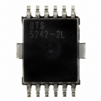
BTS5242-2L Infineon Technologies, BTS5242-2L Datasheet - Page 16

BTS5242-2L
Manufacturer Part Number
BTS5242-2L
Description
IC PWR SWITCH HISIDE PG-DSO-12-9
Manufacturer
Infineon Technologies
Series
PROFET®r
Type
High Sider
Specifications of BTS5242-2L
Package / Case
DSO-12
Input Type
Non-Inverting
Number Of Outputs
2
On-state Resistance
19 mOhm
Current - Output / Channel
6A
Current - Peak Output
50A
Voltage - Supply
4.5 V ~ 28 V
Operating Temperature
-40°C ~ 150°C
Mounting Type
Surface Mount
On Resistance (max)
0.019 Ohms
Maximum Operating Temperature
+ 150 C
Minimum Operating Temperature
- 40 C
Maximum Power Dissipation
1400 mW
Mounting Style
SMD/SMT
Supply Current
3.2 mA
Power Load Switch Type
High Side
Input Voltage
28V
Current Limit
40A
On State Resistance
0.019ohm
Thermal Protection
ESD
Power Dissipation Pd
1.4W
No. Of Outputs
2
Internal Switch
No
Rohs Compliant
Yes
Distribution Switch Case Style
SOIC
Lead Free Status / RoHS Status
Lead free / RoHS Compliant
Lead Free Status / RoHS Status
Lead free / RoHS Compliant, Lead free / RoHS Compliant
Other names
BTS5242-2LINTR
BTS52422LXT
SP000281082
BTS52422LXT
SP000281082
Available stocks
Company
Part Number
Manufacturer
Quantity
Price
Company:
Part Number:
BTS5242-2L
Manufacturer:
IT
Quantity:
12 000
Part Number:
BTS5242-2L
Manufacturer:
INFINEON/英飞凌
Quantity:
20 000
4.2.2
In case of reverse polarity, the intrinsic body diode causes power dissipation. Use following
fomular for estimation of total power dissipation
The reverse current through the power transistors has to be limited by the connected loads. The
reverse current through the ground connection has to be limited either by a resistor or by a pair of
resistor and diode. The current through sense pins IS1 and IS2 has to be limited (please refer to
maximum ratings on
4.2.3
In addition to the output clamp for inductive loads as described in
mechanism for over voltage protection. The current through the ground connection has to be
limited e.g. by a resistor.
As shown in
opens and the voltage across logic part is clamped. As a result, the ground potential rises to V
-
that potential, depending on the impedance of the connected circuitry.
Figure 12
Target Data Sheet
V
bb(AZ)
. Due to the ESD zener diodes, the potential at pin IN1, IN2 and CLA rises almost to
Reverse Polarity Protection
Over Voltage Protection
Figure
Over Voltage Protection
Page
12, in case of supply voltages greater than
IN
IS
CLA R
ZD
8). The temperature protection is not active during reverse polarity.
R
ESD
CLA
IN
P
diss(rev)
=
all channels
logic
∑
16
P
diss(rev)
V
ZD
GND
R
DS(rev)
AZ
GND
in reverse polarity mode.
Smart High-Side Power Switch
I
L
Section
V
VBB
OUT
bb(AZ)
Protection Functions
4.1.3, there is a clamp
, the power transistor
V
OUT
V1.2, 2006-08-14
BTS 5242-2L
OverVoltage .emf
bb


