BUK116-50L,118 NXP Semiconductors, BUK116-50L,118 Datasheet - Page 3
BUK116-50L,118
Manufacturer Part Number
BUK116-50L,118
Description
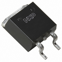
TOPFET LOGIC LVL 50V D2PAK
Manufacturer
NXP Semiconductors
Series
TOPFET™r
Type
Low Sider
Datasheet
1.BUK116-50L118.pdf
(13 pages)
Specifications of BUK116-50L,118
Input Type
Non-Inverting
Number Of Outputs
1
On-state Resistance
22 mOhm
Current - Output / Channel
50A
Current - Peak Output
200A
Mounting Type
Surface Mount
Package / Case
D²Pak, TO-263 (4 leads + tab)
Lead Free Status / RoHS Status
Lead free / RoHS Compliant
Voltage - Supply
-
Operating Temperature
-
Other names
934044320118
BUK116-50L /T3
BUK116-50L /T3
BUK116-50L /T3
BUK116-50L /T3


Philips Semiconductors
OVERVOLTAGE CLAMPING LIMITING VALUES
At a drain source voltage above 50 V the power MOSFET is actively turned on to clamp overvoltage transients.
REVERSE DIODE LIMITING VALUE
THERMAL CHARACTERISTIC
STATIC CHARACTERISTICS
T
1 The input pin must be connected to the source pin by a specified external resistance to allow the power MOSFET gate source voltage to
2 While the protection supply voltage is connected, during overvoltage clamping it is possible that the overload protection may operate at
3 Shorting the input to source with low resistance inhibits the internal overvoltage protection by preventing the power MOSFET gate source
July 1996
Logic level TOPFET
SMD version of BUK106-50L/S
SYMBOL PARAMETER
I
E
E
I
SYMBOL PARAMETER
I
SYMBOL PARAMETER
R
mb
SYMBOL PARAMETER
V
V
I
I
I
R
DRRM
DIRM
S
DSS
DSR
DSR
DSM
DRM
(CL)DSR
(CL)DSR
th j-mb
DS(ON)
= 25 ˚C unless otherwise specified
become sufficiently positive for active clamping. Refer to INPUT CHARACTERISTICS.
energies close to the limiting value. Refer to OVERLOAD PROTECTION CHARACTERISTICS.
voltage becoming positive.
Repetitive peak clamping drain current R
Non-repetitive inductive turn-off
energy
Repetitive inductive turn-off energy
Repetitive peak drain to input current
Continuous forward current
Thermal resistance
Junction to mounting base
Drain-source clamping voltage
Drain-source clamping voltage
Zero input voltage drain current V
Drain source leakage current
Drain source leakage current
Drain-source on-state
resistance
2
CONDITIONS
CONDITIONS
R
R
V
V
I
t
DM
p
-
DS
DS
DS
IS
IS
= 25 A;
3
= 100 ; I
= 100 ; I
0.01
300 s;
= 12 V; V
= 50 V; R
= 40 V; R
CONDITIONS
I
R
I
f = 250 Hz
R
CONDITIONS
T
V
DM
DM
mb
IS
IS
IS
IS
= 27 A; R
= 16 A; V
= 0 ; t
= V
= 25 ˚C;
3
100
100 ; T
IS
IS
IS
PS
D
DM
= 10 mA
= 0 V
= 100 ;
= 100 ;
0.01
= V
= 1 A; t
p
1
DD
IS
FS
mb
1 ms
= 0 V
T
100
p
20 V;
j
V
V
85 ˚C;
= 125 ˚C
IS
IS
300 s;
= 8 V
= 5 V
MIN.
MIN.
50
50
MIN.
MIN.
-
-
-
-
-
-
-
-
-
-
-
TYP.
TYP.
0.8
0.5
BUK116-50L/S
10
22
28
1
-
-
Product specification
MAX.
MAX.
50
80
50
50
1
MAX.
MAX.
100
1.0
65
70
10
20
28
35
Rev 1.000
UNIT
UNIT
mA
mJ
UNIT
UNIT
A
A
K/W
J
m
m
V
V
A
A
A
Related parts for BUK116-50L,118
Image
Part Number
Description
Manufacturer
Datasheet
Request
R

Part Number:
Description:
Buk116-50l/s Logic Level Topfet Smd Version Of Buk106-50l/s
Manufacturer:
NXP Semiconductors
Datasheet:

Part Number:
Description:
Logic level TOPFET SMD version of BUK106-50L/S
Manufacturer:
Philips Semiconductors
Datasheet:
Part Number:
Description:
NXP Semiconductors designed the LPC2420/2460 microcontroller around a 16-bit/32-bitARM7TDMI-S CPU core with real-time debug interfaces that include both JTAG andembedded trace
Manufacturer:
NXP Semiconductors
Datasheet:

Part Number:
Description:
NXP Semiconductors designed the LPC2458 microcontroller around a 16-bit/32-bitARM7TDMI-S CPU core with real-time debug interfaces that include both JTAG andembedded trace
Manufacturer:
NXP Semiconductors
Datasheet:
Part Number:
Description:
NXP Semiconductors designed the LPC2468 microcontroller around a 16-bit/32-bitARM7TDMI-S CPU core with real-time debug interfaces that include both JTAG andembedded trace
Manufacturer:
NXP Semiconductors
Datasheet:
Part Number:
Description:
NXP Semiconductors designed the LPC2470 microcontroller, powered by theARM7TDMI-S core, to be a highly integrated microcontroller for a wide range ofapplications that require advanced communications and high quality graphic displays
Manufacturer:
NXP Semiconductors
Datasheet:
Part Number:
Description:
NXP Semiconductors designed the LPC2478 microcontroller, powered by theARM7TDMI-S core, to be a highly integrated microcontroller for a wide range ofapplications that require advanced communications and high quality graphic displays
Manufacturer:
NXP Semiconductors
Datasheet:
Part Number:
Description:
The Philips Semiconductors XA (eXtended Architecture) family of 16-bit single-chip microcontrollers is powerful enough to easily handle the requirements of high performance embedded applications, yet inexpensive enough to compete in the market for hi
Manufacturer:
NXP Semiconductors
Datasheet:
Part Number:
Description:
The XA-S3 device is a member of Philips Semiconductors? XA(eXtended Architecture) family of high performance 16-bitsingle-chip microcontrollers
Manufacturer:
NXP Semiconductors
Datasheet:

Part Number:
Description:
The NXP BlueStreak LH75401/LH75411 family consists of two low-cost 16/32-bit System-on-Chip (SoC) devices
Manufacturer:
NXP Semiconductors
Datasheet:
Part Number:
Description:
The NXP LPC3130/3131 combine an 180 MHz ARM926EJ-S CPU core, high-speed USB2
Manufacturer:
NXP Semiconductors
Datasheet:
Part Number:
Description:
The NXP LPC3141 combine a 270 MHz ARM926EJ-S CPU core, High-speed USB 2
Manufacturer:
NXP Semiconductors
Part Number:
Description:
The NXP LPC3143 combine a 270 MHz ARM926EJ-S CPU core, High-speed USB 2
Manufacturer:
NXP Semiconductors

Part Number:
Description:
The NXP LPC3152 combines an 180 MHz ARM926EJ-S CPU core, High-speed USB 2
Manufacturer:
NXP Semiconductors