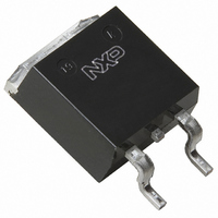
BUK116-50L,118 NXP Semiconductors, BUK116-50L,118 Datasheet - Page 4

BUK116-50L,118
Manufacturer Part Number
BUK116-50L,118
Description
TOPFET LOGIC LVL 50V D2PAK
Manufacturer
NXP Semiconductors
Series
TOPFET™r
Type
Low Sider
Datasheet
1.BUK116-50L118.pdf
(13 pages)
Specifications of BUK116-50L,118
Input Type
Non-Inverting
Number Of Outputs
1
On-state Resistance
22 mOhm
Current - Output / Channel
50A
Current - Peak Output
200A
Mounting Type
Surface Mount
Package / Case
D²Pak, TO-263 (4 leads + tab)
Lead Free Status / RoHS Status
Lead free / RoHS Compliant
Voltage - Supply
-
Operating Temperature
-
Other names
934044320118
BUK116-50L /T3
BUK116-50L /T3
BUK116-50L /T3
BUK116-50L /T3
Philips Semiconductors
OVERLOAD PROTECTION CHARACTERISTICS
With adequate protection supply
voltage TOPFET detects when one
of the overload thresholds is
exceeded.
TRANSFER CHARACTERISTICS
T
PROTECTION SUPPLY CHARACTERISTICS
T
REVERSE DIODE CHARACTERISTICS
T
1 The short circuit load protection is able to save the device providing the instantaneous on-state dissipation is less than the limiting value for
2 At the appropriate nominal protection supply voltage for each type. Refer to QUICK REFERENCE DATA.
3 The over temperature protection feature requires a minimum on-state drain source voltage for correct operation. The specified minimum I
4 During overload condition. Refer also to OVERLOAD PROTECTION LIMITING VALUES and CHARACTERISTICS.
5 The supply voltage below which the overload protection circuits will be reset.
6 The reverse diode of this type is not intended for applications requiring fast reverse recovery.
July 1996
Logic level TOPFET
SMD version of BUK106-50L/S
SYMBOL PARAMETER
E
t
T
mb
SYMBOL PARAMETER
g
I
mb
SYMBOL PARAMETER
I
I
V
V
mb
SYMBOL PARAMETER
V
t
d sc
D
PS
PSL
rr
fs
j(TO)
DS(TO)
PSR
(CL)PS
SDS
,
= 25 ˚C
= 25 ˚C unless otherwise specified
= 25 ˚C
P
ensures this condition.
DSM
, which is always the case when V
Short circuit load protection
Overload threshold energy
Response time
Over temperature protection
Threshold junction temperature from I
Forward transconductance
Drain current
Protection supply
Protection supply current
Protection reset voltage
Protection clamp voltage
Forward voltage
Reverse recovery time
4
5
DS
is less than V
Provided there is adequate input
series resistance it switches off
and remains latched off until reset
by the protection supply pin.
1
CONDITIONS
V
V
V
V
CONDITIONS
V
V
CONDITIONS
normal operation or
protection latched
T
I
CONDITIONS
I
t
not applicable
P
S
p
BUK116-50L
BUK116-50S
j
PS
DD
DD
PS
DS
DS
= 300 s
= 1.35 mA
= 20 A; V
= 150 ˚C
0.01
= V
= V
= 12 V; I
= 13 V;
= 13 V; V
= 13 V; V
DSP
D
maximum.
PSN
PSN
2.5 A
2
4
; T
IS
DM
IS
IS
= V
mb
6
3
= 25 A t
= 10 V
= 10 V
= 25 ˚C; L
PS
= V
FS
p
V
V
= 0 V;
V
PS
V
IS
300 s;
PS
IS
= 10 V
= 10 V
10 H
= 5 V
= 5 V
Refer also to OVERLOAD
PROTECTION LIMITING VALUES
and INPUT CHARACTERISTICS.
MIN.
MIN.
MIN.
MIN.
150
1.5
1.0
17
11
-
-
-
-
-
-
-
TYP.
TYP.
TYP.
TYP.
550
160
0.4
0.2
0.4
2.5
0.9
BUK116-50L/S
28
80
13
-
-
-
Product specification
MAX.
MAX.
MAX.
MAX.
0.35
1.0
3.5
1.2
-
-
-
-
-
-
-
-
-
Rev 1.000
UNIT
UNIT
UNIT
UNIT
mA
mA
mJ
ms
˚C
S
A
A
V
V
V
V
-
D


