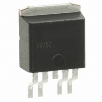
IPS521S International Rectifier, IPS521S Datasheet

IPS521S
Specifications of IPS521S
Q964168B
Available stocks
Related parts for IPS521S
IPS521S Summary of contents
Page 1
... Status feedback Open load detection Logic ground isolated from power ground Description The IPS521/IPS521S are fully protected five terminal high side switches with built in short-circuit , over- temperature, ESD protection, inductive load capability and diagnostic feedback. The output current is con- trolled when it reaches I lim value. ...
Page 2
... V cc +0 (1) o C/W) — 2.2 (1) — 10 — 4 (Human Body) — 0.5 (Machine Model) ( IPS521 — IPS521S — 1.56 -40 +150 — 300 — 50 Min. Typ. Max. Units Test Conditions — — — 60 — 35 — Units Test Conditions C=100pF, R=1500 kV C=200pF, R=0 ...
Page 3
... Output leakage current I ol Output leakage current I dg Diagnostic output leakage current leakage high threshold voltage low threshold voltage state IN positive current In hyst Input hysteresis www.irf.com C/W, ) IPS521 C/W, ) IPS521S Min. Typ — 55 — 110 C — — 5 — 56 — 0.9 — ...
Page 4
... Min. Typ 165 — — 158 Ground Vcc Out 5 Lead - D Part Number See figure 3 200 — See figure — See figure 6 Max. Units Test Conditions out = 0V See fig. 2 — — See fig See fig (Vcc PAK (SMD220) IPS521S www.irf.com ...
Page 5
... Figure 1 - Active clamp waveforms www.irf.com Over temperature 165°C Tj 158°C Level shift Current limit - Short-circuit Open load GND T clamp Vin Iout limiting Ilim. T Tsd+ Tsd- (160 ° ) Figure 2 - Protection timing diagram IPS521/IPS521S VCC 50V Charge pump driver - VOUT T shutdown cycling 5 ...
Page 6
... IPS521/IPS521S Vin Vcc 90% Vcc - 5V Vout dV/ Iout1 Eon1 Resistive load Eon2 Figure 3 - Switching times definition (turn-on) Turn on energy with a resistive or an inductive load Dg Vcc Out IN Gnd Vin Vout Rem : V load is negative during demagnetization Figure 5 - Active clamp test circuit 6 Vin 90% ...
Page 7
... Figure ds(on (V) 100 Figure 9 - Rds(on out (A) www.irf.com 200% 150% 100% 50 -50 Figure 8 - Normalized R ds(on 0 Figure 10 - Max. I out (A) Vs Load Inductance (uH) IPS521/IPS521S 0 50 100 150 ...
Page 8
... Figure 12 - Transient Thermal Impedance ( Vs Time ( Std. footprint Rthja= 60°C 125 150 o C) Figure 11b - Max load current (A) Vs Tamb ( -50 o C/W) Figure lim ( 1inch² footprint Rthja= 35°C/W 75 100 125 150 o C) IPS521S 0 50 100 150 o C) www.irf.com ...
Page 9
... Figure on, E off ( out (A) 150 125 Diag on blanking 100 Diag off blanking Figure 16 - Diag Blanking time ( out (A) (resistive load - see Fig. 6) www.irf.com 10000 1000 100 I=1. 0 Figure Load Inductance ( H) 1.00E-03 1.00E-04 1.00E-05 1.00E- IPS521/IPS521S I=Imax vs Induct.(see fig.10) (see Fig Figure (mA ( ...
Page 10
... IPS521/IPS521S Case Outline 5 Lead - TO220 Tape & Reel 5 Lead - PAK (SMD220) IRGB 01-3042 01 01-3071 00 / 01-3072 00 www.irf.com ...
Page 11
... IR JAPAN: K&H Bldg., 2F, 30-4 Nishi-Ikebukuro 3-Chome, Toshima-Ku, Tokyo, Japan 171-0021 Tel: 8133 983 0086 IR HONG KONG: Unit 308, #F, New East Ocean Centre, No. 9 Science Museum Road, Tsimshatsui East, Kowloon www.irf.com 2 PAK (SMD220) Data and specifications subject to change without notice. IPS521/IPS521S 01-3066 00 Tel (0) 20 8645 8000 Hong Kong Tel: (852) 2803-7380 3/27/2000 11 ...
Page 12
Note: For the most current drawings please refer to the IR website at: http://www.irf.com/package/ ...


