MC33982BPNA Freescale Semiconductor, MC33982BPNA Datasheet - Page 10
MC33982BPNA
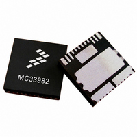
Manufacturer Part Number
MC33982BPNA
Description
IC SWITCH HI SIDE SINGLE 16-PQFN
Manufacturer
Freescale Semiconductor
Type
High Sider
Datasheet
1.MC33982BPNA.pdf
(36 pages)
Specifications of MC33982BPNA
Input Type
SPI
Number Of Outputs
1
On-state Resistance
2 mOhm
Voltage - Supply
6 V ~ 27 V
Operating Temperature
-40°C ~ 125°C
Mounting Type
Surface Mount
Package / Case
16-PQFN, 16-PowerQFN
Lead Free Status / RoHS Status
Contains lead / RoHS non-compliant
Current - Output / Channel
-
Current - Peak Output
-
Available stocks
Company
Part Number
Manufacturer
Quantity
Price

Part Number:
MC33982BPNA
Manufacturer:
FREESCALE
Quantity:
20 000


Table 4. Static Electrical Characteristics (continued)
10
33982
ELECTRICAL CHARACTERISTICS
STATIC ELECTRICAL CHARACTERISTICS
Typical values noted reflect the approximate parameter mean at T
POWER OUTPUT (CONTINUED)
CONTROL INTERFACE
Notes
Output Negative Clamp Voltage
Over-temperature Shutdown
Over-temperature Shutdown Hysteresis
Input Logic High-voltage
Input Logic Low-voltage
Input Logic Voltage Hysteresis
Input Logic Pull-down Current (SCLK, IN, SI)
RST Input Voltage Range
SO, FS Tri-state Capacitance
Input Logic Pull-down Resistor (RST) and WAKE
Input Capacitance
WAKE Input Clamp Voltage
WAKE Input Forward Voltage
SO High-state Output Voltage
FS, SO Low-state Output Voltage
SO Tri-state Leakage Current
Input Logic Pull-up Current
FSI Input Pin External Pull-down Resistance
13.
14.
15.
16.
17.
18.
Characteristics noted under conditions 4.5 V ≤ V
0.5 A < I
I
I
I
I
CS > 0.7 x V
CS, V
FSI Disabled, HS Indeterminate
FSI Enabled, HS OFF
FSI Enabled, HS ON
CL(WAKE)
CL(WAKE)
OH
OL
Guaranteed by process monitoring. Not production tested.
Upper and lower logic threshold voltage range applies to SI, CS, SCLK, RST, IN, and WAKE input signals. The WAKE and RST signals
may be supplied by a derived voltage reference to V
No hysteresis on FSI and wake pins. Parameter is guaranteed by process monitoring but is not production tested.
Input capacitance of SI, CS, SCLK, RST, and WAKE. This parameter is guaranteed by process monitoring but is not production tested.
The current must be limited by a series resistance when using voltages > 7.0 V.
Pull-up current is with CS OPEN. CS has an active internal pull-up to V
= -1.6 mA
= 1.0 mA
IN
> 0.7 x V
HS
< 2.5 mA
= -2.5 mA
< 2.0 A, Output OFF
DD
(16)
DD
(14)
(14)
(18)
(17)
Characteristic
(13)
(16)
(15)
(13)
DD
≤ 5.5 V, 6.0 V ≤ V
PWR
.
A
= 25°C under nominal conditions, unless otherwise noted.
DD
PWR
V
V
I
T
Symbol
V
SO(LEAK)
CL(WAKE)
R
R
R
SD(HYS)
R
F(WAKE)
IN(HYS)
V
.
I
V
V
C
FSOFF
V
T
R
DWN
C
FSDIS
V
I
FSON
V
DWN
SOH
RST
SOL
UP
SD
CL
SO
FS
≤ 27 V, -40°C ≤ T
IH
IL
IN
0.7 x V
0.8 x V
- 2.0
Min
160
100
100
-5.0
- 20
5.0
5.0
4.5
7.0
5.0
6.0
30
–
–
–
–
–
Analog Integrated Circuit Device Data
A
DD
DD
≤ 125°C, unless otherwise noted.
Typ
175
600
200
5.0
4.0
0.2
0.0
0.0
10
–
–
–
–
–
–
–
–
–
–
–
Freescale Semiconductor
0.2 x
1200
Max
V
-0.3
190
400
-15
5.5
0.4
5.0
1.0
20
20
20
12
14
20
14
–
DD
–
–
Unit
mV
°
°
μA
pF
kΩ
pF
μA
μA
kΩ
V
V
V
V
V
V
V
V
C
C
Related parts for MC33982BPNA
Image
Part Number
Description
Manufacturer
Datasheet
Request
R


Part Number:
Description:
Manufacturer:
Freescale Semiconductor, Inc
Datasheet:
Part Number:
Description:
Manufacturer:
Freescale Semiconductor, Inc
Datasheet:
Part Number:
Description:
Manufacturer:
Freescale Semiconductor, Inc
Datasheet:
Part Number:
Description:
Manufacturer:
Freescale Semiconductor, Inc
Datasheet:
Part Number:
Description:
Manufacturer:
Freescale Semiconductor, Inc
Datasheet:
Part Number:
Description:
Manufacturer:
Freescale Semiconductor, Inc
Datasheet:
Part Number:
Description:
Manufacturer:
Freescale Semiconductor, Inc
Datasheet:
Part Number:
Description:
Manufacturer:
Freescale Semiconductor, Inc
Datasheet:
Part Number:
Description:
Manufacturer:
Freescale Semiconductor, Inc
Datasheet:
Part Number:
Description:
Manufacturer:
Freescale Semiconductor, Inc
Datasheet:
Part Number:
Description:
Manufacturer:
Freescale Semiconductor, Inc
Datasheet:
Part Number:
Description:
Manufacturer:
Freescale Semiconductor, Inc
Datasheet:
Part Number:
Description:
Manufacturer:
Freescale Semiconductor, Inc
Datasheet:
Part Number:
Description:
Manufacturer:
Freescale Semiconductor, Inc
Datasheet: