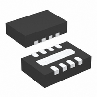
LTC4354IDDB#TRPBF Linear Technology, LTC4354IDDB#TRPBF Datasheet - Page 11

LTC4354IDDB#TRPBF
Manufacturer Part Number
LTC4354IDDB#TRPBF
Description
IC MON DIODE-OR CTRLR NEG 8DFN
Manufacturer
Linear Technology
Datasheet
1.LTC4354CS8PBF.pdf
(12 pages)
Specifications of LTC4354IDDB#TRPBF
Applications
-48V Dist Power Systems, AdvancedTCA ® Systems
Fet Type
N-Channel
Number Of Outputs
2
Internal Switch(s)
No
Delay Time - Off
700ns
Voltage - Supply
4.5 V ~ 11.75 V
Current - Supply
1.2mA
Operating Temperature
-40°C ~ 85°C
Mounting Type
Surface Mount
Package / Case
8-DFN
Lead Free Status / RoHS Status
Lead free / RoHS Compliant
Delay Time - On
-
Available stocks
Company
Part Number
Manufacturer
Quantity
Price
PACKAGE DESCRIPTIO
2.50 ±0.05
NOTE:
1. DRAWING CONFORMS TO VERSION (WECD-1) IN JEDEC PACKAGE OUTLINE M0-229
2. DRAWING NOT TO SCALE
3. ALL DIMENSIONS ARE IN MILLIMETERS
4. DIMENSIONS OF EXPOSED PAD ON BOTTOM OF PACKAGE DO NOT INCLUDE
5. EXPOSED PAD SHALL BE SOLDER PLATED
6. SHADED AREA IS ONLY A REFERENCE FOR PIN 1 LOCATION ON THE TOP AND BOTTOM OF PACKAGE
RECOMMENDED SOLDER PAD PITCH AND DIMENSIONS
1.15 ±0.05
MOLD FLASH. MOLD FLASH, IF PRESENT, SHALL NOT EXCEED 0.15mm ON ANY SIDE
0.25 ± 0.05
0.61 ±0.05
(2 SIDES)
.030 ±.005
2.20 ±0.05
(2 SIDES)
(0.203 – 0.254)
.008 – .010
TYP
NOTE:
1. DIMENSIONS IN
2. DRAWING NOT TO SCALE
3. THESE DIMENSIONS DO NOT INCLUDE MOLD FLASH OR PROTRUSIONS.
.245
MIN
0.50 BSC
RECOMMENDED SOLDER PAD LAYOUT
MOLD FLASH OR PROTRUSIONS SHALL NOT EXCEED .006" (0.15mm)
(0.254 – 0.508)
Information furnished by Linear Technology Corporation is believed to be accurate and reliable.
However, no responsibility is assumed for its use. Linear Technology Corporation makes no represen-
tation that the interconnection of its circuits as described herein will not infringe on existing patent rights.
.010 – .020
.050 BSC
0.675 ±0.05
PACKAGE
OUTLINE
(0.406 – 1.270)
(MILLIMETERS)
.016 – .050
U
8-Lead Plastic Small Outline (Narrow .150 Inch)
INCHES
× 45°
(SEE NOTE 6)
8-Lead Plastic DFN (3mm × 2mm)
(Reference LTC DWG # 05-08-1702)
(Reference LTC DWG # 05-08-1610)
TOP MARK
PIN 1 BAR
.045 ±.005
.160 ±.005
0.200 REF
0°– 8° TYP
DDB Package
S8 Package
(5.791 – 6.197)
.228 – .244
3.00 ±0.10
(2 SIDES)
(1.346 – 1.752)
(0.355 – 0.483)
.053 – .069
.014 – .019
TYP
8
1
0.75 ±0.05
2.00 ±0.10
(2 SIDES)
(4.801 – 5.004)
.189 – .197
7
2
NOTE 3
0 – 0.05
6
3
0.56 ± 0.05
(2 SIDES)
5
4
(1.270)
.050
BSC
BOTTOM VIEW—EXPOSED PAD
0.25 ± 0.05
(3.810 – 3.988)
R = 0.115
(0.101 – 0.254)
.150 – .157
.004 – .010
NOTE 3
TYP
4
SO8 0303
5
2.15 ±0.05
(2 SIDES)
LTC4354
8
1
0.50 BSC
0.38 ± 0.10
PIN 1
CHAMFER OF
EXPOSED PAD
11
(DDB8) DFN 1103
4354fb


