L6561D013TR STMicroelectronics, L6561D013TR Datasheet
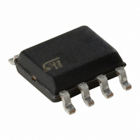
IC PFC CTRLR TRANSITION 8SOIC

L6561D013TR

Manufacturer Part Number
L6561D013TR
Description
IC PFC CTRLR TRANSITION 8SOIC
Manufacturer
STMicroelectronics
Datasheet

Specifications of L6561D013TR

Mode
Discontinuous (Transition)
Current - Startup
50µA
Voltage - Supply
11 V ~ 18 V
Operating Temperature
-25°C ~ 125°C
Mounting Type
Surface Mount
Package / Case
8-SOIC (3.9mm Width)
Maximum Operating Temperature
+ 150 C
Mounting Style
SMD/SMT
Minimum Operating Temperature
- 40 C
Supply Voltage Range
11V To 18V
Startup Current
50µA
Operating Supply Current
4mA
Digital Ic Case Style
SOIC
No. Of Pins
8
Operating Temperature Range
-40°C To +150°C
Filter Terminals
SMD
Rohs Compliant
Yes
For Use With
497-3823 - EVAL BOARD FOR HF TL BALLAST
Lead Free Status / RoHS Status
Lead free / RoHS Compliant
Frequency - Switching
-
Lead Free Status / Rohs Status
Lead free / RoHS Compliant
Other names
497-1169-2
497-1169-2
497-4582-2
E-L6561D013TR

Available stocks

Company
Part Number
Manufacturer
Quantity
Price
Part Number:
L6561D013TR
Manufacturer:
ST
Quantity:
110 000
Part Number:
L6561D013TR
Manufacturer:
INFINEON
Quantity:
40
Part Number:
L6561D013TR
Manufacturer:
ST
Quantity:
4 733
Part Number:
L6561D013TR
Manufacturer:
ST
Quantity:
310
Part Number:
L6561D013TR
Manufacturer:
ST
Quantity:
20 000
Part Number:
L6561D013TR
Manufacturer:
ST
Quantity:
11 933
Part Number:
L6561D013TR
Manufacturer:
ST
Quantity:
9 515
Part Number:
L6561D013TR
Manufacturer:
ST
Quantity:
5 185
Part Number:
L6561D013TR
0
Company:
Part Number:
L6561D013TR
Quantity:
45 000
Part Number:
L6561D013TR-7LF/
Manufacturer:
ST
0
Part Number:
L6561D013TR-8LF
Manufacturer:
ST
0
Part Number:
L6561D013TR-ST
Manufacturer:
ST
0
Part Number:
L6561D013TR.
Manufacturer:
ST
0
1
2
L6561 is the improved version of the L6560 stan-
dard Power Factor Corrector. Fully compatible
with the standard version, it has a superior perfor-
mant multiplier making the device capable of work-
ing in wide input voltage range applications (from
85V to 265V) with an excellent THD. Furthermore
the start up current has been reduced at few tens
of mA and a disable function has been implement-
ed on the ZCD pin, guaranteeing lower current
consumption in stand by mode.
Figure 2. Block Diagram
June 2004
VERY PRECISE ADJUSTABLE OUTPUT
OVERVOLTAGE PROTECTION
MICRO POWER START-UP CURRENT (50 A
TYP.)
VERY LOW OPERATING SUPPLY
CURRENT(4mA TYP.)
INTERNAL START-UP TIMER
CURRENT SENSE FILTER ON CHIP
DISABLE FUNCTION
1% PRECISION (@ T
REFERENCE VOLTAGE
TRANSITION MODE OPERATION
TOTEM POLE OUTPUT CURRENT: ±400mA
DIP-8/SO-8 PACKAGES
FEATURES
DESCRIPTION
V
INV
CC
j
= 25°C) INTERNAL
1
8
20V
R2
6
GND
2.1V
1.6V
REGULATOR
VOLTAGE
R1
V
SUPPLY 7V
INTERNAL
REF2
+
-
5
2.5V
ZCD
OVER-VOLTAGE
DETECTION
UVLO
+
-
+
-
ZERO CURRENT
DETECTOR
COMP
2
POWER FACTOR CORRECTOR
DISABLE
MULTIPLIER
Realised in mixed BCD technology, the chip gives
the following benefits:
The totem pole output stage is capable of driving
a Power MOS or IGBT with source and sink cur-
rents of ±400mA. The device is operating in tran-
sition mode and it is optimised for Electronic Lamp
Ballast application, AC-DC adaptors and SMPS.
Figure 1. Packages
Table 1. Order Codes
3
MULT
-
– micro power start up current
– 1% precision internal reference voltage
– (Tj = 25°C)
– Soft Output Over Voltage Protection
– no need for external low pass filter on the cur-
– very low operating quiescent current minimis-
R
S
+
Q
rent sense
es power dissipation
L6561D013TR
STARTER
Part Number
L6561D
L6561
5pF
40K
DRIVER
4
CS
DIP-8
D97IN547E
V
CC
7
GD
Tape & Reel
Package
SO-8
DIP-8
SO-8
L6561
REV. 16
1/13

Related parts for L6561D013TR

L6561D013TR Summary of contents

Page 1

... DETECTION INTERNAL R SUPPLY UVLO - R2 V REF2 ZERO CURRENT DETECTOR 2.1V + 1.6V - DISABLE 6 5 GND ZCD DIP-8 Part Number L6561 L6561D L6561D013TR Tape & Reel rent sense es power dissipation CS 4 40K 5pF DRIVER STARTER D97IN547E L6561 SO-8 Package DIP-8 SO-8 REV. 16 1/13 ...

Page 2

L6561 Table 2. Absolute Maximum Ratings Symbol Pin Vcc Output Totem Pole Peak Current ( INV, COMP Analog Inputs & Outputs MULT CS ...

Page 3

Table 5. Electrical Characteristics (V = 14.5V -25°C to 125°C;unless otherwise specified) CC amb Symbol Pin Parameter SUPPLY VOLTAGE SECTION V 8 Operating Range Turn-on Threshold Turn-off Threshold CC OFF Hys ...

Page 4

L6561 Table 5. Electrical Characteristics (continued 14.5V -25°C to 125°C;unless otherwise specified) CC amb Symbol Pin Parameter V 5 Lower Clamp Voltage ZCD I 5 Sink Bias Current ZCD I 5 Source Current Capability ZCD I ...

Page 5

The precision in setting the overvoltage threshold the ov- ervoltage value (for instance V = 60V ± 4.2V). 3.1 Disable function The zero current detector (ZCD) pin can be used for ...

Page 6

L6561 Figure 6. Typical Application Circuit (80W, 110VAC) BRIDGE 4 x 1N4007 + C1 FUSE 4A/250V 1 F 250V - Vac (85V to 135V) NTC (*) 120K TRANSFORMER R6 = 0.619 /2 T: core THOMSON-CSF B1ET2910A ...

Page 7

Figure 9. Demo Board (EVAL6561-80) Electrical Schematic BRIDGE C1 W04M 1 µF + FUSE 400V 4A/250V - Vac (85V to 265V Boost Inductor Spec (ITACOIL E2543/E) E25x13x7 core, 3C85 ferrite 1.5 mm gap for 0.7 mH primary ...

Page 8

L6561 Figure 11. OVP Current Threshold vs. Temperature I OVP ( -50 - Figure 12. Undervoltage Lockout Threshold vs. Temperature V CC-ON ( CC-OFF ( -25 ...

Page 9

Figure 15. Output Saturation Voltage vs. Sink Current V PIN7 ( 14.5V 2.0 1.5 1.0 0 100 200 300 Figure 16. Output Saturation Voltage vs. Source Current V PIN7 ( 14.5V V ...

Page 10

L6561 Figure 18. DIP-8 Mechanical Data & Package Dimensions mm DIM. MIN. TYP. MAX. A 3.32 a1 0.51 B 1.15 1.65 b 0.356 0.55 b1 0.204 0.304 D 10.92 E 7.95 9.75 e 2.54 e3 7.62 e4 7.62 F 6.6 ...

Page 11

Figure 19. SO-8 Mechanical Data & Package Dimensions mm DIM. MIN. TYP. MAX. A 1.35 1.75 A1 0.10 0.25 A2 1.10 1.65 B 0.33 0.51 C 0.19 0.25 4.80 5.00 ( 3.80 4.00 e 1.27 H 5.80 6.20 ...

Page 12

L6561 Table 7. Revision History Date Revision January 2004 June 2004 12/13 15 First Issue 16 Modified the Style-look in compliance with the “Corporate Technical Publications Design Guide”. Changed input of the power amplifier connected to Multiplier (Fig. 2). Description ...

Page 13

... No license is granted by implication or otherwise under any patent or patent rights of STMicroelectronics. Specifications mentioned in this publication are subject to change without notice. This publication supersedes and replaces all information previously supplied. STMicroelectronics products are not authorized for use as critical components in life support devices or systems without express written approval of STMicroelectronics ...

Related keywords