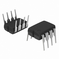
MC33262PG ON Semiconductor, MC33262PG Datasheet - Page 7

MC33262PG
Manufacturer Part Number
MC33262PG
Description
IC PFC CONTROLLER CRM 8DIP
Manufacturer
ON Semiconductor
Datasheet
1.MC34262DG.pdf
(19 pages)
Specifications of MC33262PG
Mode
Critical Conduction (CRM)
Current - Startup
250µA
Voltage - Supply
12 V ~ 28 V
Operating Temperature
-40°C ~ 105°C
Mounting Type
Through Hole
Package / Case
8-DIP (0.300", 7.62mm)
Maximum Operating Temperature
+ 105 C
Mounting Style
Through Hole
Minimum Operating Temperature
- 40 C
Lead Free Status / RoHS Status
Lead free / RoHS Compliant
Frequency - Switching
-
Lead Free Status / Rohs Status
Lead free / RoHS Compliant
Other names
MC33262PGOS
Available stocks
Company
Part Number
Manufacturer
Quantity
Price
Company:
Part Number:
MC33262PG
Manufacturer:
ON
Quantity:
5 510
Company:
Part Number:
MC33262PG
Manufacturer:
ON Semiconductor
Quantity:
8 150
Part Number:
MC33262PG
Manufacturer:
ON/安森美
Quantity:
20 000
Operating Description
blocks and protection features that are employed in modern
high performance current mode power supply controllers.
There are, however, two areas where there is a major
difference when compared to popular devices such as the
Error Amplifier
output is provided. The amplifier is a transconductance
type, meaning that it has high output impedance with
controlled voltage- - to- - current gain. The amplifier features
a typical gm of 100 mmhos (Figure 5). The noninverting
input is internally biased at 2.5 V 2.0% and is not pinned
out. The output voltage of the power factor converter is
typically divided down and monitored by the inverting
input. The maximum input bias current is - - 0.5 mA, which
can cause an output voltage error that is equal to the product
of the input bias current and the value of the upper divider
resistor R
to the Multiplier and is pinned out (Pin 2) for external loop
compensation. Typically, the bandwidth is set below 20 Hz,
so that the amplifier’s output voltage is relatively constant
over a given ac line cycle. In effect, the error amp monitors
the average output voltage of the converter over several
line cycles. The Error Amp output stage was designed to
have a relatively constant transconductance over
temperature. This allows the designer to define the
compensated bandwidth over the intended operating
temperature range. The output stage can sink and source
10 mA of current and is capable of swinging from 1.7 V to
6.4 V, assuring that the Multiplier can be driven over its
entire dynamic range.
is that the input is allowed to move independently with
respect to the output, since the compensation capacitor is
connected to ground. This allows dual usage of of the
Voltage Feedback Input pin by the Error Amplifier and by
the Overvoltage Comparator.
Overvoltage Comparator
the possibility of runaway output voltage. This condition
The MC34262, MC33262 contain many of the building
An Error Amplifier with access to the inverting input and
A key feature to using a transconductance type amplifier,
An Overvoltage Comparator is incorporated to eliminate
2
. The Error Amp output is internally connected
Line
AC
Rectifiers
Figure 18. Active Power Factor Correction Preconverter
+
High
Frequency
Bypass
Capacitor
http://onsemi.com
MC34362
PFC Preconverter
7
UC3842 series. Referring to the block diagram in
Figure 19, note that a multiplier has been added to the
current sense loop and that this device does not contain an
oscillator. The reasons for these differences will become
apparent in the following discussion. A description of each
of the functional blocks is given below.
can occur during initial startup, sudden load removal, or
during output arcing and is the result of the low bandwidth
that must be used in the Error Amplifier control loop. The
Overvoltage Comparator monitors the peak output voltage
of the converter, and when exceeded, immediately
terminates MOSFET switching. The comparator threshold
is internally set to 1.08 V
tripping during normal operation, the value of the output
filter capacitor C
peak- - to- - peak ripple less than 16% of the average dc
output. The Overvoltage Comparator input to Drive Output
turn- - off propagation delay is typically 400 ns. A
comparison of startup overshoot without and with the
Overvoltage Comparator circuit is shown in Figure 23.
Multiplier
element that enables this device to control power factor.
The ac full wave rectified haversines are monitored at Pin 3
with respect to ground while the Error Amp output at Pin 2
is monitored with respect to the Voltage Feedback Input
threshold. The Multiplier is designed to have an extremely
linear transfer curve over a wide dynamic range, 0 V to
3.2 V for Pin 3, and 2.0 V to 3.75 V for Pin 2, Figure 1. The
Multiplier output controls the Current Sense Comparator
threshold as the ac voltage traverses sinusoidally from zero
to peak line, Figure 18. This has the effect of forcing the
MOSFET on- - time to track the input line voltage, resulting
in a fixed Drive Output on- - time, thus making the
preconverter load appear to be resistive to the ac line. An
approximation of the Current Sense Comparator threshold
can be calculated from the following equation. This
equation is accurate only under the given test condition
stated in the electrical table.
A single quadrant, two input multiplier is the critical
V
CS
, Pin 4 Threshold 0.65 (V
+
Bulk
Storage
Capacitor
3
must be large enough to keep the
ref
Converter
. In order to prevent false
Pin 2
-- V
th(M)
Load
) V
Pin 3


