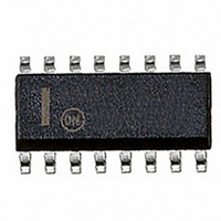
NCP1650DR2 ON Semiconductor, NCP1650DR2 Datasheet - Page 16

NCP1650DR2
Manufacturer Part Number
NCP1650DR2
Description
IC CTRLR PWR FACTOR PWM 16SOIC
Manufacturer
ON Semiconductor
Datasheet
1.NCP1650DR2G.pdf
(31 pages)
Specifications of NCP1650DR2
Mode
Continuous Conduction (CCM), Discontinuous Conduction (DCM)
Frequency - Switching
100kHz
Voltage - Supply
10 V ~ 20 V
Operating Temperature
-40°C ~ 125°C
Mounting Type
Surface Mount
Package / Case
16-SOIC (3.9mm Width)
Switching Frequency
25 KHz to 250 KHz
Maximum Operating Temperature
+ 125 C
Mounting Style
SMD/SMT
Minimum Operating Temperature
- 40 C
Lead Free Status / RoHS Status
Contains lead / RoHS non-compliant
Current - Startup
-
Lead Free Status / Rohs Status
Lead free / RoHS Compliant
Other names
NCP1650DR2OSTR
Available stocks
Company
Part Number
Manufacturer
Quantity
Price
Part Number:
NCP1650DR2G
Manufacturer:
ON/安森美
Quantity:
20 000
reference, sets the window that the instantaneous current
will modulate in, to determine when to turn the power switch
off.
a fixed frequency controller. Under normal operation, the
switch will remain on until the instantaneous value of
V
the switch will turn off.
is twice that of the line, the output filter must have poles
lower than the input current to create a reasonable DC
waveform. The output DC voltage is divided down via. an
external divider and fed back to the DC error amplifier.
Protection Features
device and circuit from overload and stressful conditions.
These include:
Output Voltage Overshoot Protection
the output voltage. Due to the slow transient response of a
PFC controller, a fast load dump can cause a large output
voltage transient to occur.
feedback and shutdown signals. Its reference is set 8%
higher than the reference used by the error amplifier. This
comparator will shutdown the output stage if the output
voltage exceeds the set level by 8%. The circuit will resume
operation once the voltage is reduced to within 8% of the set
level.
Low Line Input Protection
unit does not start under low line condition. PFC converters
typically are designed with an output voltage of 400 VDC.
To reduce this to the level of the 4.0 volt reference, a 100:1
ratio is required for the voltage divider to the FB/SD pin.
When the converter is energized, the output voltage will be
the peak line voltage. If the peak line voltage does not exceed
75 volts (0.75 volts at the FB/SD pin) the unit will not start.
This corresponds to a line voltage of 53 volts rms.
Application circuits have been provided in Figures 33
and 34 to override this feature if desired.
error(ac)
The difference between V
The switch is turned on by the oscillator, which makes this
Since the input current has a fundamental frequency that
The NCP1650 contains a number of features to protect the
An overshoot comparator has been provided to monitor
The overshoot comparator uses the same input as the
This feature uses the shutdown circuitry to assure that the
Output voltage overshoot protection
Low line input protection
Instantaneous current limit
Line frequency current limit
Maximum power limit
reaches the 4.0 volt reference level, at which time
error(ac)
and the 4.0 volt
http://onsemi.com
16
Instantaneous Current Limit
current limit feature.
instantaneous current in the inductor, and the other two are
average current waveforms. The instantaneous current
signal goes directly to the PWM and is terminated by an
internal 16 kΩ resistor. This current signal is added to the
output of the AC error amplifier and the ramp compensation
signal. The switch will conduct current until the sum of these
three signals reaches the 4.0 V reference of the inverting
input to the PWM comparator. The peak current is
determined by the value of the ramp compensation resistor
(R
Line Frequency Current Limit
current that will be required for the unit to regulate. The sum
of the input voltage from the Average Current
Compensation amplifier and the averaged current signal
from the current sense amplifier must add to the level of the
reference multiplier. The output of this multiplier is clamped
to a 4.5 maximum level. The maximum average current is set
by R
current limiting, but faster than the maximum power limit
circuit.
Maximum Power Limit
against nuisance tripping of circuit breakers or other input
power restrictions. It should be understood that boost
regulators by design, can not be short circuit limited.
Operation of the power limiting circuit will reduce the
output voltage only to the level where it is equal to the peak
of the input line voltage. At this point, the rectified line
voltage will continue to provide output voltage through line
frequency rectification by means of the series rectifier
diode.
power multiplier. By multiplying the instantaneous input
voltage (AC input signal, pin 5) and the instantaneous input
current (averaged current sense amplifier output), the actual
input power is accurately calculated.
converts the power to a filtered DC level. The power error
amplifier has a reference set at 2.5 volts. If the output of the
power multiplier reaches 2.5 volts, the power error amplifier
takes control of the loop via the ORing network and will
regulate a constant power output within the limits of the
power stage. It should be understood that once the output
voltage is reduced to a level equal to the peak of the input
voltage, the converter can no longer control the output
power.
resistor at pin 10 and the P
The fastest protection available is a cycle- -by- -cycle
The current sense amplifier has three outputs. One is the
The output of the reference multiplier determines the
This form of protection is slower than the cycle- -by- -cycle
The NCP1650 can limit the output power to protect
The input power of the converter is calculated by the
The power multiplier has a very low frequency pole which
The output power level is set by combination of the I
13
) and the current shunt.
10
.
max
resistor at pin 9.
avg


