SI1869DH-T1-E3 Vishay, SI1869DH-T1-E3 Datasheet - Page 2
SI1869DH-T1-E3
Manufacturer Part Number
SI1869DH-T1-E3
Description
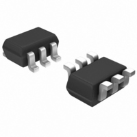
IC LOAD SW LVL SHIFT 20V SC70-6
Manufacturer
Vishay
Type
High Side Switchr
Datasheet
1.SI1869DH-T1-E3.pdf
(6 pages)
Specifications of SI1869DH-T1-E3
Transistor Polarity
N and P-Channel
Number Of Outputs
1
Rds (on)
165 mOhm
Internal Switch(s)
Yes
Current Limit
1.2A
Voltage - Input
1.8 ~ 20 V
Operating Temperature
-55°C ~ 150°C
Mounting Type
Surface Mount
Package / Case
SC-70-6, SC-88, SOT-363
Minimum Operating Temperature
- 55 C
Configuration
Dual
Drain-source Breakdown Voltage
20 V
Continuous Drain Current
1.2 A
Power Dissipation
1000 mW
Maximum Operating Temperature
+ 150 C
Mounting Style
SMD/SMT
Module Configuration
Dual
Continuous Drain Current Id
700mA
Drain Source Voltage Vds
-20V
On Resistance Rds(on)
303mohm
Rds(on) Test Voltage Vgs
4.5V
Lead Free Status / RoHS Status
Lead free / RoHS Compliant
Lead Free Status / RoHS Status
Lead free / RoHS Compliant, Lead free / RoHS Compliant
Other names
SI1869DH-T1-E3TR
Available stocks
Company
Part Number
Manufacturer
Quantity
Price
Company:

Part Number:
SI1869DH-T1-E3
Manufacturer:
VISHAY
Quantity:
23 000
Part Number:
SI1869DH-T1-E3
Manufacturer:
VISHAY/威世
Quantity:
20 000


Si1869DH
Vishay Siliconix
FUNCTIONAL BLOCK DIAGRAM
Notes:
a. Surface mounted on FR4 board.
b. V
c. Pulse test: pulse width ≤ 300 µs, duty cycle ≤ 2 %.
Stresses beyond those listed under “Absolute Maximum Ratings” may cause permanent damage to the device. These are stress ratings only, and functional operation
of the device at these or any other conditions beyond those indicated in the operational sections of the specifications is not implied. Exposure to absolute maximum
rating conditions for extended periods may affect device reliability.
www.vishay.com
2
Ordering Information: Si1869DH-T1-E3 (Lead (Pb)-free)
R2
D2
D2
ABSOLUTE MAXIMUM RATINGS T
Parameter
Drain-Source Voltage (D2-S2)
Input Voltage
ON/OFF Voltage
Load Current
Continuous Intrinsic Diode Conduction
Maximum Power Dissipation
Operating Junction and Storage Temperature Range
ESD Rating, MIL-STD-883D Human Body Model (100 pF, 1500 Ω)
THERMAL RESISTANCE RATINGS
Parameter
Maximum Junction-to-Ambient (Continuous Current)
Maximum Junction-to-Foot (Q2)
SPECIFICATIONS T
Parameter
OFF Characteristics
Reverse Leakage Current
Diode Forward Voltage
ON Characteristics
Input Voltage Range
Drain to Source Breakdown Voltage
On-Resistance (P-Channel) at 1 A
On-State (P-Channel) Drain-Current
IN
= 20 V, V
1
2
3
Top View
SC70-6
ON/OFF
6
5
4
Si1869DH-T1-GE3 (Lead (Pb)-free and Halogen-free)
= 8 V, T
a
R1, C1
ON/OFF
S2
J
A
= 25 °C.
= 25 °C unless otherwise noted
a
Marking Code
Symbol
R
VC XX
I
V
DS(on)
V
D(on)
V
I
FL
SD
DS
IN
Part # Code
A
a
V
V
= 25 °C, unless otherwise noted
IN-OUT
IN-OUT
V
V
V
Lot T raceability
and Date Code
ON/OFF
ON/OFF
ON/OFF
≤ 0.2 V, V
≤ 0.3 V, V
V
V
Continuous
Pulsed
IN
GS
= 1.5 V, V
= 1.5 V, V
= 1.5 V, V
Test Conditions
= 8 V, V
= 0 V, I
I
S
b, c
IN
IN
= - 0.4 A
= 5 V, V
= 3 V, V
IN
IN
IN
ON/OFF
D
a, b
= - 250 µA
= 4.5 V, I
= 2.5 V, I
= 1.8 V, I
ON/OFF
ON/OFF
= 0 V
ON/OFF
D
D
D
V
Symbol
Symbol
T
ON/OFF
R
R
J
ESD
= 1.2 A
= 1.0 A
= 0.7 A
V
V
P
, T
I
thJA
thJF
I
DS
= 1.5 V
= 1.5 V
S
IN
L
S2
D
stg
4
5
Typical
Min.
- 20
0.4
1.8
1
1
100
44
Si1869DH
- 55 to 150
R2
Limit
± 1.2
- 0.4
1
- 20
± 3
1.0
20
8
2
0.132
0.177
0.242
Typ.
0.6
S10-0792-Rev. C, 05-Apr-10
Maximum
Q2
Q1
Document Number: 73449
125
55
2, 3
6
0.165
0.222
0.303
Max.
1.1
20
1
D2
R1,
C1
°C/W
Unit
Unit
kV
°C
W
V
A
Unit
µA
Ω
V
V
A
Related parts for SI1869DH-T1-E3
Image
Part Number
Description
Manufacturer
Datasheet
Request
R

Part Number:
Description:
Load Switch With Level
Manufacturer:
Vishay
Datasheet:
Part Number:
Description:
357-036-542-201 CARDEDGE 36POS DL .156 BLK LOPRO
Manufacturer:
Vishay
Datasheet:
Part Number:
Description:
357-036-542-201 CARDEDGE 36POS DL .156 BLK LOPRO
Manufacturer:
Vishay
Datasheet:
Part Number:
Description:
357-036-542-201 CARDEDGE 36POS DL .156 BLK LOPRO
Manufacturer:
Vishay
Datasheet:
Part Number:
Description:
357-036-542-201 CARDEDGE 36POS DL .156 BLK LOPRO
Manufacturer:
Vishay
Datasheet:
Part Number:
Description:
357-036-542-201 CARDEDGE 36POS DL .156 BLK LOPRO
Manufacturer:
Vishay
Datasheet:
Part Number:
Description:
357-036-542-201 CARDEDGE 36POS DL .156 BLK LOPRO
Manufacturer:
Vishay
Datasheet:
Part Number:
Description:
357-036-542-201 CARDEDGE 36POS DL .156 BLK LOPRO
Manufacturer:
Vishay
Datasheet:
Part Number:
Description:
357-036-542-201 CARDEDGE 36POS DL .156 BLK LOPRO
Manufacturer:
Vishay
Datasheet:
Part Number:
Description:
357-036-542-201 CARDEDGE 36POS DL .156 BLK LOPRO
Manufacturer:
Vishay
Datasheet:
Part Number:
Description:
357-036-542-201 CARDEDGE 36POS DL .156 BLK LOPRO
Manufacturer:
Vishay
Datasheet:
Part Number:
Description:
357-036-542-201 CARDEDGE 36POS DL .156 BLK LOPRO
Manufacturer:
Vishay
Datasheet:
Part Number:
Description:
357-036-542-201 CARDEDGE 36POS DL .156 BLK LOPRO
Manufacturer:
Vishay
Datasheet:
Part Number:
Description:
357-036-542-201 CARDEDGE 36POS DL .156 BLK LOPRO
Manufacturer:
Vishay
Datasheet: