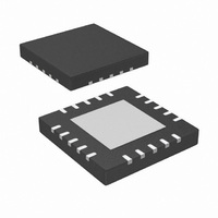
IR3507MTRPBF International Rectifier, IR3507MTRPBF Datasheet

IR3507MTRPBF
Specifications of IR3507MTRPBF
Related parts for IR3507MTRPBF
IR3507MTRPBF Summary of contents
Page 1
NOT RECOMMENDED FOR NEW DESIGNS DESCRIPTION The IR3507 Phase IC combined with an IR XPhase3 implement power solutions for the latest high performance CPUs and ASICs. The “Control” IC provides overall system control and interfaces with any number of “Phase” ...
Page 2
... NOT RECOMMENDED FOR NEW DESIGNS ORDERING INFORMATION Part Number IR3507MTRPBF * IR3507MPBF * Samples only ABSOLUTE MAXIMUM RATINGS Stresses beyond those listed under “Absolute Maximum Ratings” may cause permanent damage to the device. These are stress ratings only and functional operation of the device at these or any other conditions beyond those indicated in the operational sections of the specifications are not implied. Operating Junction Temperature… ...
Page 3
NOT RECOMMENDED FOR NEW DESIGNS RECOMMENDED OPERATING CONDITIONS FOR RELIABLE OPERATION WITH MARGIN 8.0V ≤ V ≤ 28V, 4.75V ≤ V ≤ 7.5V CCL ≤ PHSIN ≤1.5MHz ELECTRICAL CHARACTERISTICS The electrical characteristics involve the spread of values guaranteed ...
Page 4
NOT RECOMMENDED FOR NEW DESIGNS REPLACEMENT PRODUCT – IR3507ZPBF PARAMETER PWM Comparator PWM Ramp Slope Vin=12V Input Offset Voltage Note 1 EAIN Bias Current 0 ≤ EAIN ≤ 3V Minimum Pulse Width Note 1 Minimum GATEH Turn-off Time Current Sense ...
Page 5
NOT RECOMMENDED FOR NEW DESIGNS REPLACEMENT PRODUCT – IR3507ZPBF PARAMETER Body Brake Comparator Threshold Voltage with EAIN decreasing Threshold Voltage with EAIN increasing Hysteresis Propagation Delay OVP Comparator OVP Threshold Propagation Delay Synchronous Rectification Disable Comparator Threshold Voltage Negative Current ...
Page 6
NOT RECOMMENDED FOR NEW DESIGNS REPLACEMENT PRODUCT – IR3507ZPBF PIN DESCRIPTION PIN# PIN SYMBOL PIN DESCRIPTION 1 IOUT Output of the Current Sense Amplifier is connected to this pin through a 3kΩ resistor. Voltage on this pin is equal to ...
Page 7
NOT RECOMMENDED FOR NEW DESIGNS REPLACEMENT PRODUCT – IR3507ZPBF SYSTEM THEORY OF OPERATION System Description The system consists of one control IC and a scalable array of phase converters, each requiring one phase IC. The control IC communicates with the ...
Page 8
NOT RECOMMENDED FOR NEW DESIGNS REPLACEMENT PRODUCT – IR3507ZPBF Frequency and Phase Timing Control The oscillator is located in the Control IC and the system clock frequency is programmable from 250kHz to 9MHZ by an external resistor. The control IC ...
Page 9
NOT RECOMMENDED FOR NEW DESIGNS REPLACEMENT PRODUCT – IR3507ZPBF An additional advantage of the architecture is that differences in ground or input voltage at the phases have no effect on operation since the PWM ramps are referenced to VDAC. Figure ...
Page 10
NOT RECOMMENDED FOR NEW DESIGNS REPLACEMENT PRODUCT – IR3507ZPBF Usually the resistor Rcs and capacitor Ccs are chosen so that the time constant of Rcs and Ccs equals the time constant of the inductor which is the inductance L over ...
Page 11
NOT RECOMMENDED FOR NEW DESIGNS REPLACEMENT PRODUCT – IR3507ZPBF share loop is much slower than that of the voltage loop and the two loops do not interact. For proper current sharing the output of current sense amplifier should note exceed ...
Page 12
NOT RECOMMENDED FOR NEW DESIGNS REPLACEMENT PRODUCT – IR3507ZPBF A synchronous rectification disable comparator is used to detect converter CSIN- pin voltage, which represents local converter output voltage. If the voltage is below 75% of VDAC and negative current is ...
Page 13
NOT RECOMMENDED FOR NEW DESIGNS REPLACEMENT PRODUCT – IR3507ZPBF PSI ASSERT PHSIN PSI GATEH GATEL Debugging Mode If CSIN+ pin is pulled up to VCCL voltage, IR3507 enters into debugging mode. Both drivers are pulled low and IOUT output is ...
Page 14
NOT RECOMMENDED FOR NEW DESIGNS REPLACEMENT PRODUCT – IR3507ZPBF Over Voltage Protection (OVP) The IR3507 includes over-voltage protection that turns on the low side MOSFET to protect the load in the event of a shorted high-side MOSFET, converter out of ...
Page 15
NOT RECOMMENDED FOR NEW DESIGNS REPLACEMENT PRODUCT – IR3507ZPBF LAYOUT GUIDELINES The following layout guidelines are recommended to reduce the parasitic inductance and resistance of the PCB layout; therefore, minimizing the noise coupled to the IC. • Dedicate at least ...
Page 16
NOT RECOMMENDED FOR NEW DESIGNS REPLACEMENT PRODUCT – IR3507ZPBF PCB Metal and Component Placement • Lead land width should be equal to nominal part lead width. The minimum lead to lead spacing should be ≥ 0.2mm to minimize shorting. • ...
Page 17
NOT RECOMMENDED FOR NEW DESIGNS REPLACEMENT PRODUCT – IR3507ZPBF Solder Resist • The solder resist should be pulled away from the metal lead lands and center pad by a minimum of 0.06mm. The solder resist mis-alignment is a maximum of ...
Page 18
NOT RECOMMENDED FOR NEW DESIGNS REPLACEMENT PRODUCT – IR3507ZPBF Stencil Design • The stencil apertures for the lead lands should be approximately 80% of the area of the lead lands. Reducing the amount of solder deposited will minimize the occurrence ...
Page 19
PACKAGE INFORMATION 20L MLPQ ( Body) – θ IR WORLD HEADQUARTERS: 233 Kansas St., El Segundo, California 90245, USA Tel: (310) 252-7105 Visit us at www.irf.com for sales contact information. Page ...


