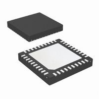
LP3971SQ-O509/NOPB National Semiconductor, LP3971SQ-O509/NOPB Datasheet - Page 23

LP3971SQ-O509/NOPB
Manufacturer Part Number
LP3971SQ-O509/NOPB
Description
IC PMU FOR APPL PROCESSORS 40LLP
Manufacturer
National Semiconductor
Series
PowerWise®r
Datasheet
1.LP3971SQ-B510NOPB.pdf
(50 pages)
Specifications of LP3971SQ-O509/NOPB
Applications
Processor
Current - Supply
60µA
Voltage - Supply
2.7 V ~ 5.5 V
Operating Temperature
-40°C ~ 85°C
Mounting Type
Surface Mount
Package / Case
40-LLP
Lead Free Status / RoHS Status
Lead free / RoHS Compliant
Other names
LP3971SQ-O509
LP3971SQ-O509
LP3971SQ-O509TR
LP3971SQ-O509
LP3971SQ-O509TR
I
I
The data on SDA line must be stable during the HIGH period
of the clock signal (SCL). In other words, state of the data line
can only be changed when CLK is LOW.
I
START and STOP bits classify the beginning and the end of
the I
transitioning from HIGH to LOW while SCL line is HIGH.
STOP condition is defined as the SDA transitioning from LOW
to HIGH while SCL is HIGH. The I
TRANSFERRING DATA
Every byte put on the SDA line must be eight bits long, with
the most significant bit (MSB) being transferred first. The
number of bytes that can be transmitted per transfer is unre-
stricted. Each byte of data has to be followed by an acknowl-
edge bit. The acknowledge related clock pulse is generated
by the master. The transmitter releases the SDA line (HIGH)
during the acknowledge clock pulse. The receiver must pull
down the SDA line during the 9th clock pulse, signifying an
I
2
2
2
MSB
2
C DATA VALIDITY
C START AND STOP CONDITIONS
C CHIP ADDRESS - 7h'34
C Compatible Interface
2
ADR6
C session. START condition is defined as SDA signal
Bit7
0
ADR5
Bit6
1
2
C master always generates
ADR4
Bit5
1
ADR3
Bit4
0
23
START and STOP bits. The I
after START condition and free after STOP condition. During
data transmission, I
conditions. First START and repeated START conditions are
equivalent, function-wise.
acknowledge. A receiver which has been addressed must
generate an acknowledge after each byte has been received.
After the START condition, a chip address is sent by the I
master. This address is seven bits long followed by an eighth
bit which is a data direction bit (R/W). The LP3971 address is
34h. For the eighth bit, a “0” indicates a WRITE and a “1”
indicates a READ. The second byte selects the register to
which the data will be written. The third byte contains data to
write to the selected register.
ADR2
Bit3
1
2
ADR1
C master can generate repeated START
Bit2
0
20180715
20180714
2
C bus is considered to be busy
ADR0
Bit1
0
www.national.com
R/W
R/W
Bit0
2
C


