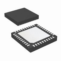
LP3971SQ-O509/NOPB National Semiconductor, LP3971SQ-O509/NOPB Datasheet - Page 25

LP3971SQ-O509/NOPB
Manufacturer Part Number
LP3971SQ-O509/NOPB
Description
IC PMU FOR APPL PROCESSORS 40LLP
Manufacturer
National Semiconductor
Series
PowerWise®r
Datasheet
1.LP3971SQ-B510NOPB.pdf
(50 pages)
Specifications of LP3971SQ-O509/NOPB
Applications
Processor
Current - Supply
60µA
Voltage - Supply
2.7 V ~ 5.5 V
Operating Temperature
-40°C ~ 85°C
Mounting Type
Surface Mount
Package / Case
40-LLP
Lead Free Status / RoHS Status
Lead free / RoHS Compliant
Other names
LP3971SQ-O509
LP3971SQ-O509
LP3971SQ-O509TR
LP3971SQ-O509
LP3971SQ-O509TR
Designation
Reset Value
Register
Address
LP3971 I
I
INTERRUPT STATUS REGISTER (ISR) 8H'02
INTERRUPT STATUS REGISTER (ISR) 8H'02 DEFINITIONS
2
Bit
C CONTROL REGISTERS
8h'0B
8h'0E
8h'2A
8h'2B
8h'3A
8h'3B
8h'02
8h'07
8h'10
8h'11
8h'12
8h'13
8h'20
8h'23
8h'24
8h'25
8h'29
8h'32
8h'33
8h'34
8h'38
8h'39
7
6
5
4
3
2
Bit
Access
—
R
R
R
R
R
2
Register
L21VCR
L43VCR
BOVEN
BOVSR
LDOEN
LDOVS
L5VCR
B1TV1
B1TV2
B2TV1
B2TV2
B3TV1
B3TV2
C Register Definitions
Name
SCR1
BBCC
SCR2
B1RC
B2RC
B3RC
V
BFR
ISR
CC
1
WUP3
WUP2
Name
T125
GPI2
GPI1
—
T100
7
0
Read/
Write
R/W
R/W
R/W
R/W
R/W
R/W
R/W
R/W
R/W
R/W
R/W
R/W
R/W
R/W
R/W
R/W
R/W
R/W
R/W
R
R
R
Reserved
Status bit for thermal warming PMIC T>125°C
0 = PMIC Temp. <125°C
1 = PMIC Temp. >125°C
Status bit for the input read in from GPIO 2 when set as Input
0 = GPI2 Logic Low
1 = GPI2 Logic High
Status bit for the input read in from GPIO 1 when set as Input
0 = GPI1 Logic Low
1 = GPI1 Logic High
PWR_ON Pin Long Pulse Wake Up Status
0 = 1 No wake up event
1 = Long pulse wake up event
PWR_ON Pin Short Pulse Wake Up Status
0 = No wake up event
1 = Short pulse wake up event
T125
6
0
Interrupt Status Register A
System Control Register 1
Backup Battery Charger Control Register
System Control Register 2
Buck Output Voltage Enable Register
Buck Output Voltage Status Register
LDO Output Voltage Enable Register
LDO Output Voltage Status Register
Voltage Change Control Register 1
Buck 1 Target Voltage 1 Register
Buck 1 Target Voltage 2 Register
Buck 1 Ramp Control
Buck 2 Target Voltage 1 Register
Buck 2 Target Voltage 2 Register
Buck 2 Voltage Ramp Control
Buck 3 Target Voltage 1 Register
Buck 3 Target Voltage 2 Register
Buck 3 Voltage Ramp Control
Buck Function Register
LDO2 & 1 Voltage Control Registers
LDO4 & LDO3 Voltage Control Registers
LDO5 Voltage Control Registers
GPI2
5
0
GPI1
25
4
0
Register Description
WUP3
Description
3
0
WUP2
2
0
WUPT
1
0
www.national.com
WUPS
0
0


