ISL6532CRZ Intersil, ISL6532CRZ Datasheet
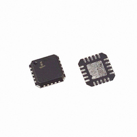
IC CTRLR PWM 2CHAN DDR 20QFN

ISL6532CRZ

Manufacturer Part Number
ISL6532CRZ
Description
IC CTRLR PWM 2CHAN DDR 20QFN
Manufacturer
Intersil
Datasheet

Specifications of ISL6532CRZ

Applications
Memory, DDR/DDR2 Regulator
Current - Supply
5.25mA
Operating Temperature
0°C ~ 70°C
Mounting Type
Surface Mount
Package / Case
20-QFN
Lead Free Status / RoHS Status
Lead free / RoHS Compliant
Voltage - Supply
-

Available stocks

Company
Part Number
Manufacturer
Quantity
Price
Part Number:
ISL6532CRZ
Manufacturer:
INTERSIL
Quantity:
20 000
ACPI Regulator/Controller for
Dual Channel DDR Memory Systems
The ISL6532 provides a complete ACPI compliant power
solution for up to 4 DIMM dual channel DDR/DDR2 memory
systems. Included are both a synchronous buck controller
and integrated LDO to supply V
S0/S1 states and standby current during S3 state. During
Run mode, a fully integrated sink-source regulator generates
an accurate (V
need for a negative supply. A buffered version of the V
reference is provided as V
The switching PWM controller drives two N-Channel
MOSFETs in a synchronous-rectified buck converter
topology. The synchronous buck converter uses voltage-
mode control with fast transient response. Both the switching
regulator and integrated standby LDO provide a maximum
static regulation tolerance of
temperature ranges. The output is user-adjustable by means
of external resistors down to 0.8V.
Switching the memory core output between the PWM
regulator and the standby LDO during state transitions is
accomplished smoothly via the internal ACPI control
circuitry. The NCH signal provides synchronized switching of
a backfeed blocking switch during the transitions eliminating
the need to route 5V Dual to the memory supply.
An integrated soft-start feature brings V
a controlled manner when returning to S0/S1 state from
S4/S5 or mechanical off states. During S0 the PGOOD signal
indicates that all supplies are within spec and operational.
Each output is monitored for under and over-voltage events.
Current limiting is included on the V
regulators. Thermal shutdown is integrated.
Pinout
5VSBY
VDDQ
GND
VTT
VTT
DDQ
1
2
3
4
5
ISL6532 (QFN) TOP VIEW
/2) high current V
20
6
19
7
®
REF
GND
±
1
21
18
.
2% over line, load, and
8
DDQ
17
9
Data Sheet
TT
with high current during
TT
16
10
DDQ
and V
voltage without the
15
14
13
12
11
into regulation in
DDQ
NCH
PGOOD
GND
COMP
FB
standby
DDQ
1-888-INTERSIL or 321-724-7143
CAUTION: These devices are sensitive to electrostatic discharge; follow proper IC Handling Procedures.
/2
Features
• Generates 2 Regulated Voltages
• ACPI Compliant Sleep State Control
• Integrated V
• PWM Controller Drives Low Cost N-Channel MOSFETs
• 250kHz Constant Frequency Operation
• Tight Output Voltage Regulation
• 5V or 3.3V Down Conversion
• Fully-Adjustable Outputs with Wide Voltage Range: Down
• Simple Single-Loop Voltage-Mode PWM Control Design
• Fast PWM Converter Transient Response
• Over Current Protection and Under/Over-Voltage
• Integrated Thermal Shutdown Protection
• QFN Package Option
• Pb-free available
Applications
• Single and Dual Channel DDR Memory Power Systems in
• Graphics cards - GPU and memory supplies
• ASIC power supplies
• Embedded processor and I/O supplies
• DSP supplies
Ordering Information
PART NUMBER
ISL6532CR
ISL6532CRZ
(See Note)
*Add “-T” suffix to part number for tape and reel packaging.
NOTE: Intersil Pb-free products employ special Pb-free material sets; molding
compounds/die attach materials and 100% matte tin plate termination finish, which
is compatible with both SnPb and Pb-free soldering operations. Intersil Pb-free
products are MSL classified at Pb-free peak reflow temperatures that meet or
exceed the Pb-free requirements of IPC/JEDEC J Std-020B.
- Synchronous Buck PWM Controller with Standby LDO
- 3A Integrated Sink/Source Linear Regulator with
- Glitch-free Transitions During State Changes
- Both Outputs:
to 0.8V supports DDR and DDR2 Specifications
Monitoring of Both Outputs
- QFN Compliant to JEDEC PUB95 MO-220 QFN - Quad
- QFN Near Chip Scale Package Footprint; Improves
ACPI compliant PCs
Accurate V
Flat No Leads - Product Outline
PCB Efficiency, Thinner in Profile
All other trademarks mentioned are the property of their respective owners.
|
Intersil (and design) is a registered trademark of Intersil Americas Inc.
July 2004
Copyright © Intersil Americas Inc. 2002-2004. All Rights Reserved
REF
DDQ
TEMP. RANGE
±
Buffer
/2 Divider Reference.
2% Over Temperature
0 to 70
0 to 70
(
o
C)
20 Ld 6x6 QFN
20 Ld 6x6 QFN
(Pb-free)
PACKAGE
ISL6532
FN9112.3
L20.6x6
L20.6x6
DWG. #
PKG.

Related parts for ISL6532CRZ

ISL6532CRZ Summary of contents

Page 1

... PGOOD PART NUMBER 13 GND ISL6532CR 12 COMP ISL6532CRZ (See Note *Add “-T” suffix to part number for tape and reel packaging. NOTE: Intersil Pb-free products employ special Pb-free material sets; molding compounds/die attach materials and 100% matte tin plate termination finish, which is compatible with both SnPb and Pb-free soldering operations ...

Page 2

Block Diagram P3V3SBY VDDQ S3 REGULATOR VDDQ(2) VTTSNS VTT REG VTT(2) DISABLE { R U VREF_IN { R L UV/OV VREF_OUT SLP_S3# SLP_S5# 5VSBY VOLTAGE REFERENCE 0.800V 0.680V (-15%) 0.920V (+15%) 5V POR S3 SLEEP, SOFT-START, PGOOD, AND FAULT PWM ...

Page 3

Simplified Power System Diagram SLP_S3 SLP_S5 5VSBY/3V3SBY Typical Application - 5V or 3.3V Input PGOOD V DDQ V REF VTT 3 ISL6532 12V 5VSBY SLEEP STATE LOGIC PWM CONTROLLER STANDBY LDO ISL6532 VTT REGULATOR 5VSBY +12V ...

Page 4

Typical Application - Input From 5V Dual PGOOD V DDQ V REF VTT 4 ISL6532 5VSBY +12V +3. S3# SLP_S3 NCH S5# SLP_S5 VREF_OUT VREF_IN UGATE C SS ISL6532 LGATE VTT VDDQ VTT VDDQ ...

Page 5

Absolute Maximum Ratings 5VSBY . . . . . . . . . . . . . . . . . . . . . . . . . . . . . . . . . GND - 0.3V ...

Page 6

Electrical Specifications Recommended Operating Conditions, Unless Otherwise Noted. Refer to Block and Simplified Power System Diagrams and Typical Application Schematics (Continued) PARAMETER PWM CONTROLLER GATE DRIVERS UGATE and LGATE Source UGATE and LGATE Sink NCH BACKFEED CONTROL NCH Current Sink ...

Page 7

FB (Pin 11) and COMP (Pin 12) The V switching regulator employs a single voltage DDQ control loop the negative input to the voltage loop error amplifier. The positive input of the error amplifier is connected to a ...

Page 8

ISL6532 starts an internal counter. Following a cold start or any subsequent S5 state, state transitions are ignored until the system enters S0/S1. None of the regulators will begin the soft start procedure until the 5V Standby bus has ...

Page 9

Active to Shutdown (S0 to S4/S5 Transition) When the system transitions from active, S0, state to shutdown, S4/S5, state, the ISL6532 IC disables all regulators and forces the PGOOD pin and the NCH pin LOW. Over/Under Voltage Protection . Both ...

Page 10

Dedicate one solid layer, usually a middle layer of the PC board, for a ground plane and make all critical component ground connections with vias to this layer. Dedicate another solid layer as a power plane ...

Page 11

OSC Modulator Break Frequency Equations 1 = ------------------------------------------ - = ------------------------------------------- - ESR 2π x ESR 2π ...

Page 12

High frequency decoupling capacitors should be placed as close to the power pins of the load as physically possible. Be careful not to add inductance in the circuit board wiring that could cancel the usefulness of these low inductance components. ...

Page 13

When sourcing current, the upper MOSFET realizes most of the switching losses. The lower switch realizes most of the switching losses when the converter is sinking current (see the equations below). These ...

Page 14

... Accordingly, the reader is cautioned to verify that data sheets are current before placing orders. Information furnished by Intersil is believed to be accurate and reliable. However, no responsibility is assumed by Intersil or its subsidiaries for its use; nor for any infringements of patents or other rights of third parties which may result from its use ...

Related keywords