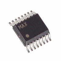
MAX1602EEE+ Maxim Integrated Products, MAX1602EEE+ Datasheet

MAX1602EEE+
Specifications of MAX1602EEE+
Related parts for MAX1602EEE+
MAX1602EEE+ Summary of contents
Page 1
... Information PART TEMP. RANGE MAX1602EEE -40°C to +85°C Pin Configuration appears on last page. ________________________________________________________________ Maxim Integrated Products For free samples & the latest literature: http://www.maxim-ic.com, or phone 1-800-998-8800 Power-Switching Network ____________________________Features Supports a Single PC Card/CardBus Socket 1A, 0.25Ω Max 3.3V VCC Switch 1A, 0.25Ω ...
Page 2
Single-Channel CardBus and PCMCIA VCC/VPP Power-Switching Network ABSOLUTE MAXIMUM RATINGS Inputs/Outputs to GND (VX, VY, VCC) (Note 1) ..........................................-0.3V, +6V VPP Input/Output to GND (12IN, VPP) (Note 1) ............................................-0.3V, +15V Logic Inputs to GND (A0VCC, A1VCC, A0VPP, A1VPP) (Note 1)........................................-0.3V, ...
Page 3
Single-Channel CardBus and PCMCIA VCC/VPP ELECTRICAL CHARACTERISTICS (continued) (VY = 3.3V 5V, 12IN = 12V 0°C to +85°C, unless otherwise noted. Typical values are PARAMETER Output Sink Current Output Leakage Current Output Propagation ...
Page 4
Single-Channel CardBus and PCMCIA VCC/VPP Power-Switching Network ELECTRICAL CHARACTERISTICS (VY = 3.3V 5V, 12IN = 12V -40°C to +85°C, unless otherwise noted.) A PARAMETER POWER-SUPPLY SECTION VX, VY Input Voltage Range 12IN VY falling edge, hysteresis ...
Page 5
Single-Channel CardBus and PCMCIA VCC/VPP __________________________________________Typical Operating Characteristics (VY = 3.3V 5V, 12IN = 12V +25°C, unless otherwise noted.) A VCC SWITCHING (RISE VCC ( CONTROL INPUT 5 (V) 0 500 s/div ...
Page 6
Single-Channel CardBus and PCMCIA VCC/VPP Power-Switching Network _____________________________Typical Operating Characteristics (continued) (VY = 3.3V 5V, 12IN = 12V +25°C, unless otherwise noted.) A VCC CURRENT LIMITING 4 2 VCC (V) 0 2ms/div ...
Page 7
Single-Channel CardBus and PCMCIA VCC/VPP _____________________________Typical Operating Characteristics (continued) (VY = 3.3V 5V, 12IN = 12V +25°C, unless otherwise noted.) A 12IN ON-RESISTANCE vs. CURRENT 680 675 670 665 660 655 650 645 640 0 20 ...
Page 8
Single-Channel CardBus and PCMCIA VCC/VPP Power-Switching Network ______________________________________________________________Pin Description PIN NAME 1 GND Ground 2 12IN +12V Supply Voltage Input 3 VPP VPP Output VCC VCC Output. Connect all four VCC pins together ...
Page 9
Single-Channel CardBus and PCMCIA VCC/VPP _________Logic Truth Tables (cont.) Table 3. “Databook” Code, CODE = Mid-Supply (VY/2) A1VCC A0VCC AVPP A0VPP ...
Page 10
Single-Channel CardBus and PCMCIA VCC/VPP Power-Switching Network independent of resistive and capacitive loads (see rise- time photos in the Typical Operating Characteristics ). Fall times are a function of loading, and are compensat internal circuitry. Power savings is ...
Page 11
Single-Channel CardBus and PCMCIA VCC/VPP TO PC CARD SOCKET VCC VPP SOCKET INTERFACE 82365SL DF MAX1602 +3. A:VPP_EN0 A0VPP A:VPP_EN1 A1VPP +5V VX A:VCC_EN0 A0VCC 12IN +12V CODE A:VCC_EN1 A1VCC GND Figure 3. Application with Intel Interface ______________________________________________________________________________________ ...
Page 12
... Maxim reserves the right to change the circuitry and specifications without notice at any time. implied. Maxim reserves the right to change the circuitry and specifications without notice at any time. 12 __________________Maxim Integrated Products, 120 San Gabriel Drive, Sunnyvale, CA 94086 (408) 737-7600 12 __________________Maxim Integrated Products, 120 San Gabriel Drive, Sunnyvale, CA 94086 (408) 737-7600 © ...


