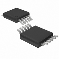
LT3420EMS-1 Linear Technology, LT3420EMS-1 Datasheet

LT3420EMS-1
Specifications of LT3420EMS-1
Available stocks
Related parts for LT3420EMS-1
LT3420EMS-1 Summary of contents
Page 1
... DONE pin signals that the capacitor is fully charged. The LT3420/LT3420-1 are available in 10-Lead MSOP and (3mm × 3mm) DFN packages. , LTC and LT are registered trademarks of Linear Technology Corporation. All other trademarks are the property of their respective owners. *Protected by U.S. Patents including 6518733. 320V ...
Page 2
... Switching RREF – 0.2V (Note 4) RFB BAT V = 1.1V, Not Switching RREF 3.3V CHARGE IN ORDER PART NUMBER 10 C LT3420EMS T 9 CHARGE LT3420EMS-1 8 DONE 7 SEC PART MARKING = 45°C/W JC LTYH LTAJG = V unless otherwise noted. (Note 3) CC MIN TYP MAX UNITS ● 2.2 2 ...
Page 3
ELECTRICAL CHARACTERISTICS temperature range, otherwise specifications are at T PARAMETER Primary Side Current Limit Secondary Side Current Limit Leakage Blanking Pulse Width Refresh Timer Charge/Discharge Current Refresh Timer Upper Threshold Refresh Timer Lower Threshold Switch V CESAT Switch Leakage Current ...
Page 4
LT3420/LT3420 TYPICAL PERFOR A CE CHARACTERISTICS Graphs apply to both the LT3420 and LT3420-1 unless otherwise noted. Output Voltage in Refresh Mode, LT3420-1 335 330 325 320 315 310 305 FIGURE 2 CIRCUIT 300 V = 3.3V CC ...
Page 5
W U TYPICAL PERFOR A CE CHARACTERISTICS Graphs apply to both the LT3420 and LT3420-1 unless otherwise noted. Efficiency for Figure 2 Circuit, LT3420 25° 3. ...
Page 6
LT3420/LT3420 CTIO S R (Pin 1): Reference Resistor Pin. Place a resistor (R2) REF from the R pin to GND recommended. REF V (Pin 2): Battery Voltage Input. This pin should be BAT ...
Page 7
W BLOCK DIAGRA S V BAT C1 DONE 8 REFRESH TIMER C3 BLOCK ENABLE Q Q MASTER LATCH S R ONE- CHARGE 9 SHOT CHIP ENABLE BAT C1 DONE 8 ...
Page 8
LT3420/LT3420-1 U OPERATIO Overview The following text focuses on the operation of the LT3420. The operation of the LT3420-1 is nearly identical with the differences discussed at the end of this section. The LT3420 uses an adaptive on-time/off-time control scheme ...
Page 9
U OPERATIO I SW 1A/DIV I SEC 200mA/DIV V SW 20V/DIV 2µs/DIV Figure 6a. Switching Waveforms with V = 100V 3.3V OUT CC BAT that the peak current 1.4A and ...
Page 10
... Choosing the Right Transformer The flyback transformer plays a key role in any LT3420/ LT3420-1 application. A poorly designed transformer can result in inefficient operation. Linear Technology Corpora- tion has worked with a number of transformer manufactur- ers to develop specific transformers for use with the LT3420/LT3420-1. These predesigned transformers are sufficient for a large majority of the applications that may be encountered ...
Page 11
U U APPLICATIO S I FOR ATIO must be taken into account for the dynamic blocking voltage capabilities of the LT3420/LT3420-1. The dynamic blocking voltage capability of both parts is 38V. Table 1 summarizes the various breakdown voltages of the ...
Page 12
LT3420/LT3420 APPLICATIO S I FOR ATIO efficiency of the circuit. In addition, the effective capaci- tance on the primary is largely dominated by the actual secondary capacitance. This is simply a result of any secondary capacitance being multiplied ...
Page 13
U U APPLICATIO S I FOR ATIO CAPACITOR SELECTION The V and V decoupling capacitors should be multi- BAT CC layer ceramic type with X5R or X7R dielectric. This insures adequate decoupling across wide ambient temperature ranges. A good quality ...
Page 14
LT3420/LT3420 APPLICATIO S I FOR ATIO risk of drawing too much current from the battery. The input current to the LT3420/LT3420-1 circuit can be adjusted by driving the CHARGE pin with a PWM (pulse width modulation) signal. The ...
Page 15
U U APPLICATIO S I FOR ATIO BOARD LAYOUT The high voltage operation of the LT3420/LT3420-1 demands careful attention to board layout. You will not get advertised performance with careless layout. Fig- ures 11 and 12 show the recommended component ...
Page 16
LT3420/LT3420-1 U TYPICAL APPLICATIO S Professional Charger uses Multiple LT3420 Circuits in Parallel to Charge Large Photoflash Capacitors Quickly DANGER HIGH VOLTAGE OPERATION BY HIGH VOLTAGE TRAINED PERSONEL ONLY C1, C2, C4, C5, C6, C7: 4.7µF, X5R or X7R, 10V ...
Page 17
U TYPICAL APPLICATIO S LT3420 Photoflash Charging Circuit Uses Small Transformer DANGER HIGH VOLTAGE OPERATION BY HIGH VOLTAGE TRAINED PERSONEL ONLY 1. 2.5V TO 10V CHARGE C1: 4.7µF, X5R or X7R, 6.3V C2: 4.7µF, X5R or X7R, 10V ...
Page 18
LT3420/LT3420-1 PACKAGE DESCRIPTIO 5.23 (.206) MIN 0.305 ± 0.038 (.0120 ± .0015) TYP RECOMMENDED SOLDER PAD LAYOUT 0.254 (.010) GAUGE PLANE 0.18 (.007) NOTE: 1. DIMENSIONS IN MILLIMETER/(INCH) 2. DRAWING NOT TO SCALE 3. DIMENSION DOES NOT INCLUDE MOLD FLASH, ...
Page 19
... RECOMMENDED SOLDER PAD PITCH AND DIMENSIONS TOP MARK (SEE NOTE 6) Information furnished by Linear Technology Corporation is believed to be accurate and reliable. However, no responsibility is assumed for its use. Linear Technology Corporation makes no represen- tation that the interconnection of its circuits as described herein will not infringe on existing patent rights Package 10-Lead Plastic DFN (3mm × ...
Page 20
... Step-Up DC/DC Converter with Integrated Schottky and Output Disconnect LTC3467 1. 1.3MHz, High Efficiency Step-Up SW DC/DC Converter LTC3468/LTC3468-1/ Photoflash Capacitor Charger in ThinSOT LTC3468-2 ThinsSOT is a trademark of Linear Technology Corporation. Linear Technology Corporation 20 1630 McCarthy Blvd., Milpitas, CA 95035-7417 (408) 432-1900 FAX: (408) 434-0507 ● 320V 4 D1 ...


