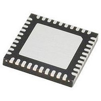
IR3523MTRPBF International Rectifier, IR3523MTRPBF Datasheet - Page 26

IR3523MTRPBF
Manufacturer Part Number
IR3523MTRPBF
Description
IC XPHASE3 CTLR VR11.1 40-MLPQ
Manufacturer
International Rectifier
Series
XPhase3™r
Datasheet
1.IR3523MTRPBF.pdf
(37 pages)
Specifications of IR3523MTRPBF
Applications
Processor
Current - Supply
10mA
Voltage - Supply
4.75 V ~ 7.5 V
Operating Temperature
0°C ~ 100°C
Mounting Type
Surface Mount
Package / Case
40-MLPQ
Ic Function
Dual Output Control IC
Supply Voltage Range
4.75V To 7.5V
Operating Temperature Range
0°C To +150°C
Digital Ic Case Style
MLPQ
No. Of Pins
40
Controller Type
XPhase
Rohs Compliant
Yes
Package
40-Lead MLPQ
Circuit
X-Phase Control IC
Switch Freq (khz)
250kHz to 1.5MHz
Pbf
PbF Option Available
Lead Free Status / RoHS Status
Lead free / RoHS Compliant
VDAC Slew Rate Programming Capacitor C
The slew rate of VDACx down-slope SR
(5), where I
down-slope. The resistor R
Over Current Setting Resistor R
The inductor DC resistance is utilized to sense the inductor current. The copper wire of inductor has a constant
temperature coefficient of 3850 ppm/° C, and therefore the maximum inductor DCR can be calculated from (7),
where R
T
The total input offset voltage (V
(V
sense resistor R
The over current limit is set by the external resistor R
limit. I
CHARACTERISTICS Table. G
over average current in each phase and can be calculated from (10).
VCCL Programming Resistor R
Since VCCL voltage is proportional to the MOSFET gate driver loss and inversely proportional to the
MOSFET conduction loss, the optimum voltage should be chosen to maximize the converter efficiency. VCCL
linear regulator consists of an external NPN transistor, a ceramic capacitor and a programmable resistor
divider. Pre-select R
L
CS_OFST)
_
ROOM
OCSET
Page 26 of 37
L_MAX
respectively.
SINK
of the amplifier itself and that created by the amplifier input bias current flowing through the current
is the bias current of OCSET pin and can be calculated with the equation in the ELECTRICAL
and R
CS
is the sink current of VDAC pin. The slew rate of VDAC up-slope is three times greater that of
.
VCCLFB1
L_ROOM
V
R
R
K
R
CS
VCCLFB
L
OCSET
P
VDAC
_
_
=
MAX
, and calculate R
TOFST
(
CS
V
are the inductor DCR at maximum temperature T
=
2
I
is used to compensate VDAC circuit and is determined by (6).
=
VCCLFB1
CS_TOFST
[
−
=
is the gain of the current sense amplifier. K
OCSET
R
I
R
C
=
V
VDAC
LIMIT
R
L
VDAC
O
VCCL
V
n
VCCLFB
_
)
CS
ROOM
∗
V
_
DOWN
=
∗
O
=
OFST
R
I
0
and R
−
1
O
/(
) of current sense amplifier in phase ICs is the sum of input offset
SR
5 .
L
∗
*
. 1
L
_
/
I
1 [
. 1
VCCLFB2
+
23
MAX
n
SINK
DOWN
+
∗
VDAC
23
+
can be programmed by the external capacitor C
V
3
I
3850
VCCLFB2
2 .
I
C
CSIN
∗
∗
VDAC
∗
1 (
f
10
and Resistor R
+
SW
+
*
∗
from (11).
−
10
2
K
OCSET
15
∗
R
P
−
) 2
CS
6
)
∗
+
(
V
T
CS
L
as defined in (9). I
_
_
MAX
TOFST
VDAC
−
T
]
∗
L
G
_
ROOM
CS
/
P
I
OCSET
)]
is the ratio of inductor peak current
LIMIT
L_MAX
is the required over current
(5)
(6)
(7)
(8)
(9)
(10)
(11)
and room temperature
June 20, 2008
VDAC
IR3523
as defined in


