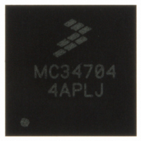
MC34704AEP Freescale Semiconductor, MC34704AEP Datasheet - Page 32

MC34704AEP
Manufacturer Part Number
MC34704AEP
Description
IC POWER MANAGEMENT 56-QFN
Manufacturer
Freescale Semiconductor
Datasheet
1.MC34704BEPR2.pdf
(54 pages)
Specifications of MC34704AEP
Applications
Processor
Current - Supply
86mA
Voltage - Supply
2.7 V ~ 5.5 V
Operating Temperature
-20°C ~ 85°C
Mounting Type
Surface Mount
Package / Case
56-QFN
Output Voltage
5 V
Input Voltage
2.7 V to 5.5 V
Switching Frequency
750 KHz to 2 MHz
Mounting Style
SMD/SMT
Number Of Outputs
8
Lead Free Status / RoHS Status
Lead free / RoHS Compliant
Switching frequency for REG6, 7 & 8
in 250 kHz steps. On the 34704B, FSW2 is just for REG8
since REG6 and 7 do not exist in this device.
Shutdown Hold (Delay) Time
processor to program the shutdown delay time period
details
Programming 34704 response to under-voltage/over-
voltage conditions on each regulator
over-voltage/under-voltage condition:
is detected, the concerned output shuts down and a register
is flagged to alert the processor.
is detected, the concerned output will not shutdown, but the
register is flagged to alert the processor. Then, the processor
32
34704
FUNCTIONAL DEVICE OPERATION
LOGIC COMMANDS AND REGISTERS
OPTION
F
34704 assigns 2 bits to program F
The 34704 assigns 2 bits (SDDELAY[1:0]) for the
Please refer to the /ONOFF pin description for more
There are two responses that can be programmed for an
Response A: When an over-voltage (under-voltage) event
Response B: When an over-voltage/under-voltage event
SW2
2
3
4
can be selected to be between 250 kHz and 1.0 MHz
500kHz (Default)
Shutdown Delay
1.0sec (Default)
MSB
1000kHz
0
1
1
250kHz
750kHz
0.5sec
1.5sec
2.0sec
FSW2
LSB
1
0
1
REG5, REG6, and REG7 ramp up together
Then REG6 and REG7 ramp up together
REG5 and REG6 ramp up together first.
MSB
MSB
SW2
0
0
1
1
0
0
1
1
(F
Then ramp up REG7
GRPC/E ENABLED
REG5 ramps up first
SW2
LSB
LSB
0
1
0
1
0
1
0
1
[1:0])
can decide whether to shutdown the output or not. In the
mean time, the concerned output control loop will be
attempting to correct the error.
page 30
corresponds to each regulator.
Dynamic Voltage Scaling for each regulator
dynamically with 2.5% step size. The total range of
adjustability will vary depending on each regulator to
accommodate different operating environments. Some
regulators will utilize the full range of -20.00% to +17.50%
and some regulators will only use the range of ±10.00%. For
details, see each regulator’s section. Each 2.5% step takes
50 μs before moving to the next step. REG8 only performs
DVS when in voltage regulation mode.
monitoring will not be active. In addition to that, these faults
will be masked and not active for a DVS settling time period
equal to 1ms. This DVS settling time will start after the
DVSSTAT register is flagged indicating that the DVS cycle is
done. This is to ensure that during DVS and soft start alike
the output will not be tripped due to a momentary over-
voltage or under-voltage fault. This is the same for Response
A and Response B of the over-voltage/under-voltage fault
monitoring.
Voltage Scaling for each regulator (DVSSETx[3:0]) where x
corresponds to each regulator.
See Output Over-voltage/Under-voltage Monitoring on
Response A and Response B share the same flag bit
34704 assigns 1 bit for this function (OVUVSETx) where x
The customer can adjust each regulator’s output
During DVS, the Over-voltage and Under-voltage
34704 assigns 4 bits register to program the Dynamic
for more details.
REG5, REG6, and REG7 ramp down together
REG5, REG6 and REG7 ramp down together
Then REG5 and REG6 ramp down together
OV/UV Response
A (Default)
Analog Integrated Circuit Device Data
REG7 ramps down first.
GRPC/E DISABLED
B
Freescale Semiconductor
bit
0
1


