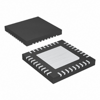
MAX1702BETX+ Maxim Integrated Products, MAX1702BETX+ Datasheet - Page 11

MAX1702BETX+
Manufacturer Part Number
MAX1702BETX+
Description
IC PWR MNG TRPL OUT 36-TQFN
Manufacturer
Maxim Integrated Products
Datasheet
1.MAX1702BETX.pdf
(19 pages)
Specifications of MAX1702BETX+
Applications
Processor
Voltage - Supply
2.6 V ~ 5.5 V
Operating Temperature
-40°C ~ 85°C
Mounting Type
Surface Mount
Package / Case
36-TQFN Exposed Pad
Lead Free Status / RoHS Status
Lead free / RoHS Compliant
Current - Supply
-
Lead Free Status / Rohs Status
Lead free / RoHS Compliant
1, 9, 13, 18,
19, 26, 27,
31, 35
PIN
10
11
12
14
15
16
17
2
3
4
5
6
7
8
COMP1
NAME
PGM3
GND
GND
INP1
N.C.
ON2
PG1
REF
RSO
LX1
DBI
______________________________________________________________________________________
LBI
MR
IN
Triple-Output Power-Management IC for
No Connection. These pins are not internally connected.
Low-Battery Input. Connect a resistive voltage-divider from the battery voltage to LBI to set the low-
battery threshold. LBI threshold voltage is 1.235V.
Dead-Battery Input. Connect a resistive voltage-divider from the battery voltage to DBI to set the
dead-battery voltage threshold. When the voltage at DBI is below the 1.25V threshold, the MAX1702B
is turned off and draws only 5µA from the battery.
REG2 On/Off Input. Drive ON2 high to turn on REG2, drive it low to turn it off. When enabled, the
MAX1702B soft-starts REG2, when disabled, the output of REG2 is internally discharged to PG2.
REG3 Regulation Voltage-Control Input. Connect PGM3 to IN, REF, or GND to set the REG3 output
regulation voltage. Connect PGM3 to GND for 1.8V, REF for 2.5V, and IN for 3.3V.
Connect Pin 6 to Pin 8
Reference Output. Output of the 1.25V reference. Bypass REF to GND with a 0.1µF or greater
capacitor.
Analog Ground. Connect GND to a local analog ground plane with no high-current paths. GND
should be connected to the main ground plane at a single point as close to the IC and the IN bypass
capacitor as possible. Connect the ground of the low-noise components, such as resistive voltage-
dividers and reference bypass capacitor to the analog ground plane.
Analog Supply Input. Bypass IN to GND with a 1µF or greater low-ESR capacitor.
Reset Output. RSO is low (sinks current to GND) during initial startup or while the manual reset input,
MR, is asserted. RSO remains low for 65.5ms after all regulators are in regulation or after MR is
deasserted. RSO is an open-drain output. RSO remains high when REG2 is turned off. The RSO line
maintains a valid low output for IN as low as 1V.
REG1 Power Ground. Connect PG1 directly to a power ground plane. Connect PG1, PG2, PG3 and
GND together at a single point as close to the IC as possible.
REG1 Power-Switching Node. Connect the external inductor of the REG1 output LC filter from LX1 to
OUT1 (see the Inductor Selection section).
REG1 Power Input. Bypass INP1 to PG1 with a 1.0µF or greater low-ESR capacitor. INP1, INP2, INP3,
and IN must be connected together externally. A single 4.7µF capacitor can be used for INP1, INP2,
and INP3.
Manual Reset Input. A momentary low on MR forces RSO to go low. RSO remains low as long as MR
is low, and returns high 65.5ms after MR returns high and all output voltages are in regulation.
REG1 Compensation Node. Connect a series resistor and capacitor from COMP1 to GND in parallel
with a 33pF capacitor to compensate REG1 (see the Compensation and Stability section).
Microprocessor-Based Systems
FUNCTION
Pin Description
11


