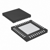
MAX1702BETX+ Maxim Integrated Products, MAX1702BETX+ Datasheet - Page 16

MAX1702BETX+
Manufacturer Part Number
MAX1702BETX+
Description
IC PWR MNG TRPL OUT 36-TQFN
Manufacturer
Maxim Integrated Products
Datasheet
1.MAX1702BETX.pdf
(19 pages)
Specifications of MAX1702BETX+
Applications
Processor
Voltage - Supply
2.6 V ~ 5.5 V
Operating Temperature
-40°C ~ 85°C
Mounting Type
Surface Mount
Package / Case
36-TQFN Exposed Pad
Lead Free Status / RoHS Status
Lead free / RoHS Compliant
Current - Supply
-
Lead Free Status / Rohs Status
Lead free / RoHS Compliant
Triple-Output Power-Management IC for
Microprocessor-Based Systems
Table 1. Suggested Inductors
The inductor current becomes discontinuous if I
decreases to LIR/2 from the output current value used
to determine L
The input capacitor reduces the current peaks drawn
from the battery or input power source and reduces
switching noise in the IC. The impedance of the input
capacitor at the switching frequency should be less
than that of the input source so high-frequency switch-
ing currents do not pass through the input source but
instead are shunted through the input capacitor.
The input capacitor must meet the ripple-current require-
ment (I
capacitor RMS current is:
The output capacitor is required to keep the output-volt-
age ripple small and to ensure regulation control-loop
stability. The output capacitor must have low impedance
at the switching frequency. Ceramic capacitors are rec-
ommended. The output ripple is approximately:
See the Compensation and Stability section for a dis-
cussion of the influence of output capacitance and ESR
on regulation control-loop stability.
The capacitor voltage rating must exceed the maximum
applied capacitor voltage. Consult the manufacturer’s
specifications for proper capacitor derating. Avoid Y5V
and Z5U dielectric types due to their huge voltage and
temperature coefficients of capacitance and ESR. X7R
and X5R dielectric types are recommended.
16
Coilcraft
Coilcraft
Sumida
Sumida
Sumida
MANUFACTURER
V
RIPPLE
______________________________________________________________________________________
RMS
I
) imposed by the switching currents. The input
RMS
≈
LIR I
IDEAL
=
×
I
LOAD
OUT MAX
.
Output Capacitor Selection
PART NUMBER
CDRH4D28-4R7
CDRH5D18-4R1
(
Input Capacitor Selection
LPT1606-472
DO1606
V
CR43
)
OUT
×
ESR
(
V
V
IN
IN
−
+
V
OUT
2
×
f
)
INDUCTANCE (µH)
OSC
1
×
C
4.7
4.7
4.7
4.1
4.7
OUT
OUT
The low-battery and dead-battery detector trip points
can be set by adjusting the resistor values of the
divider string (R1, R2, and R3) in Figure 1 according to
the following:
1) Choose R3 to be less than 250kΩ
2) R1 = R3
3) R2 = R3
where V
battery voltage, and V
High switching frequencies and large peak currents
make PC board layout a very important part of design.
Good design minimizes excessive EMI on the feedback
paths and voltage gradients in the ground plane, both
of which can result in instability or regulation errors.
Connect the inductor, input filter capacitor, and output
filter capacitor as close together as possible, and keep
their traces short, direct, and wide. Connect their
ground pins to a single common power ground plane.
The external voltage-feedback network should be very
close to the FB pin, within 0.2in (5mm). Keep noisy
traces (from the LX pin, for example) away from the
voltage-feedback network; also, keep them separate,
using grounded copper. Connect GND and PG_ pins
together at a single point, as close as possible to the
MAX1702B. Refer to the MAX1702B evaluation kit for a
PC board layout example.
TRANSISTOR COUNT: 10,890
PROCESS: BiCMOS
ESR (mW)
240 (max)
108.7
120
56
57
BL
is the low-battery voltage, V
✕
✕
V
(V
SATURATION CURRENT
BL
TH
Setting the Battery Detectors
PC Board Layout and Routing
✕
✕
(1 - V
V
TH
BL
1.32
1.95
1.15
= 1.235V.
(A)
1.2
1.2
/V
TH
BD
Chip Information
/V
BD
- 1)
)
BD
DIMENSIONS
6.5 x 5.3 x 2.0
5.3 x 5.3 x 2
5.5 x 5.5 x 2
4.5 x 4 x 3.5
4.6 x 5 x 3
is the dead-
(mm)


