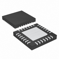
MAX16050ETI+ Maxim Integrated Products, MAX16050ETI+ Datasheet

MAX16050ETI+
Specifications of MAX16050ETI+
Related parts for MAX16050ETI+
MAX16050ETI+ Summary of contents
Page 1
... Storage Systems Networking Systems Typical Operating Circuit appears at end of data sheet. PART TEMP RANGE -40°C to +85°C MAX16050ETI+ -40°C to +85°C MAX16051ETI+ + Denotes lead-free/RoHS-compliant package Exposed pad. ________________________________________________________________ Maxim Integrated Products For pricing, delivery, and ordering information, please contact Maxim Direct at 1-888-629-4642, or visit Maxim’ ...
Page 2
Voltage Monitors/Sequencer Circuits with Reverse-Sequencing Capability ABSOLUTE MAXIMUM RATINGS (All voltages referenced to GND.) V .........................................................................-0.3V to +30V CC REM, OUT_, DISC_.................................................-0.3V to +30V RESET, SHDN, SET_, FAULT, EN_HOLD, EN, DELAY, OV_OUT, ABP, TIMEOUT, SEQ_...........................-0.3V to +6V CP_OUT.........................................................-0. ...
Page 3
Voltage Monitors/Sequencer Circuits with ELECTRICAL CHARACTERISTICS (continued 2.7V to 13.2V ABP A PARAMETER SYMBOL DELAY, TIMEOUT Output Source Current DELAY, TIMEOUT Threshold V Voltage DIGITAL INPUTS/OUTPUTS SHDN, FAULT, EN_HOLD ...
Page 4
Voltage Monitors/Sequencer Circuits with Reverse-Sequencing Capability ( +25°C, unless otherwise noted ABP A SUPPLY CURRENT vs. SUPPLY VOLTAGE 750 700 650 600 T = +85° +25°C A ...
Page 5
Voltage Monitors/Sequencer Circuits with ( +25°C, unless otherwise noted ABP A OV_OUT LOW VOLTAGE vs. SINK CURRENT 0.8 0.7 0.6 0.5 0.4 0.3 0.2 0 ...
Page 6
Voltage Monitors/Sequencer Circuits with Reverse-Sequencing Capability PIN NAME MAX16050 MAX16051 GND 3 3 ABP SET4 6 6 OUT4 7 7 DISC4 8 8 SET3 9 9 OUT3 10 10 ...
Page 7
Voltage Monitors/Sequencer Circuits with PIN NAME MAX16050 MAX16051 18 18 SET1 OV_OUT 19 19 RESET 20 20 FAULT 21 21 SHDN DELAY 24 24 TIMEOUT 25 — SEQ1 26 — SEQ2 27 — SEQ3 28 28 ...
Page 8
Voltage Monitors/Sequencer Circuits with Reverse-Sequencing Capability CHARGE PUMP CP_OUT COMP SET1–SET4 (SET1–SET5) COMP EN COMP EN_HOLD SEQ1–SEQ3 (MAX16050 ONLY ARE FOR MAX16051 ONLY. 8 _______________________________________________________________________________________ V CC INTERNAL V /UVLO CC V REF CONTROL LOGIC ABP GND TIMEOUT ...
Page 9
Voltage Monitors/Sequencer Circuits with V TH_EN EN SHDN t DELAY RESET REM Figure 1. Sequencing Timing Diagram with Reverse Order Power-Down Using SHDN _______________________________________________________________________________________ Reverse-Sequencing Capability DELAY DELAY ...
Page 10
Voltage Monitors/Sequencer Circuits with Reverse-Sequencing Capability V TH_EN EN SHDN t DELAY RESET REM Figure 2. Sequencing Timing Diagram with Simultaneous Order Power-Down Using EN 10 ______________________________________________________________________________________ DELAY ...
Page 11
Voltage Monitors/Sequencer Circuits with FAULT RESET REM Figure 3. Sequencing Timing Diagram During a System Fault ______________________________________________________________________________________ Reverse-Sequencing Capability t FAULT-PW t DELAY V TH_PL V TH_PL 11 ...
Page 12
Voltage Monitors/Sequencer Circuits with Reverse-Sequencing Capability EN EN_HOLD CONNECTED TO REM OF THE SECOND Figure 4. Power-Down Characteristics when REM of the Second IC is Connected to EN_HOLD of the First IC 12 ______________________________________________________________________________________ ... ...
Page 13
Voltage Monitors/Sequencer Circuits with Detailed Description The MAX16050 monitors voltages (Figure 5) with the ability to sequence voltages, while the MAX16051 monitors voltages with the ability to sequence ...
Page 14
Voltage Monitors/Sequencer Circuits with Reverse-Sequencing Capability When all of these conditions are met, the device starts the power-sequencing process by turning on OUT1–OUT_ in the sequence order. The sequence delay between each OUT_ is the time required for the power-supply ...
Page 15
Voltage Monitors/Sequencer Circuits with Charge-Pump Output (CP_OUT) The MAX16050/MAX16051 feature an on-chip charge pump that drives its output voltage to 5V above V and it can be used as a pullup voltage to drive one or more external n-channel MOSFETs ...
Page 16
Voltage Monitors/Sequencer Circuits with Reverse-Sequencing Capability Enable Hold Input ( EN_HOLD ) When EN_HOLD is low, a high-to-low transition on SHDN ignored. EN_HOLD must be high for SHDN disable the device. This feature ...
Page 17
Voltage Monitors/Sequencer Circuits with Daisy-Chaining the MAX16050/MAX16051 The MAX16050/MAX16051 can be daisy-chained to sequence and monitor a large number of voltages (Figure 7). When a fault occurs on any of the monitored inputs, FAULT goes low, signaling a fast power-down. ...
Page 18
Voltage Monitors/Sequencer Circuits with Reverse-Sequencing Capability V BUS DC-DC EN DC-DC EN DC- MAX16050 GND ABP EN_HOLD PULL SHDN LOW TO INITIATE A REVERSE ORDER SHUTDOWN OF ALL 8 SUPPLIES Figure 7. Daisy-Chaining Two Devices ...
Page 19
Voltage Monitors/Sequencer Circuits with Reverse-Sequencing Capability V BUS DC-DC EN DC- GND ON SHDN OFF ______________________________________________________________________________________ Typical Operating Circuit DC-DC EN CP_OUT RESET MAX16050 OV_OUT FAULT REM ...
Page 20
Voltage Monitors/Sequencer Circuits with Reverse-Sequencing Capability Pin Configurations (continued) TOP VIEW SHDN 22 DELAY 23 TIMEOUT 24 25 DISC5 MAX16051 26 OUT5 27 SET5 * CP_OUT THIN QFN ...
Page 21
... Maxim cannot assume responsibility for use of any circuitry other than circuitry entirely embodied in a Maxim product. No circuit patent licenses are implied. Maxim reserves the right to change the circuitry and specifications without notice at any time. Maxim Integrated Products, 120 San Gabriel Drive, Sunnyvale, CA 94086 408-737-7600 ____________________ 21 © 2008 Maxim Integrated Products ...


