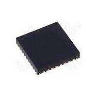
MAX15048ETJ+ Maxim Integrated Products, MAX15048ETJ+ Datasheet - Page 21

MAX15048ETJ+
Manufacturer Part Number
MAX15048ETJ+
Description
IC CTRLR PWM STP-DN TRIPL 32WQFN
Manufacturer
Maxim Integrated Products
Datasheet
1.MAX15048ETJ.pdf
(31 pages)
Specifications of MAX15048ETJ+
Applications
Power Supply Controller, Sequencer
Voltage - Supply
4.7 V ~ 23 V
Current - Supply
6mA
Operating Temperature
-40°C ~ 85°C
Mounting Type
Surface Mount
Package / Case
32-WQFN Exposed Pad
Number Of Outputs
3
Output Voltage
5 V
Input Voltage
4.7 V to 23 V
Supply Current
6 mA
Switching Frequency
200 KHz
Mounting Style
SMD/SMT
Maximum Operating Temperature
+ 85 C
Minimum Operating Temperature
- 40 C
Lead Free Status / RoHS Status
Lead free / RoHS Compliant
Voltage - Input
-
Lead Free Status / Rohs Status
Lead free / RoHS Compliant
Use the following equations to calculate the required
ESR, ESL, and capacitance value during a load step:
where I
load step, t
troller, and f
of system (see the Compensation Design Guidelines
section).
The MAX15048/MAX15049 use a valley current-sense
method for current limiting. The valley current-limit
threshold (V
The voltage drop across the low-side MOSFET due to its
on-resistance is used to sense the inductor current. The
voltage drop (V
the valley point and at I
R
I
peak inductor current.
The R
Calculate the R
junction temperature at full load using its data sheet. To
compensate for this temperature variation, the current-
limit circuitry has a temperature coefficient of 3333ppm/NC.
This allows the valley current-limit threshold (V
track and partially compensate for the increase in the
R
temperature.
LOAD
DS(ON)
DS(ON)
DS(ON)
is the rated load current, and DI
V
STEP
VALLEY
is the on-resistance of the low-side MOSFET,
of the synchronous MOSFET with increasing
RESPONSE
LIM
CO
is the load step, t
of the MOSFET varies with temperature.
C
) is internally set at 69mV (typ).
VALLEY
DS(ON)
is the closed-loop crossover frequency
=
OUT
ESL
______________________________________________________________________________________
t
R
RESPONSE
DS(ON)
ESR
=
=
) across the low-side MOSFET at
is the response time of the con-
I
LOAD
∆
of the MOSFET at its operating
STEP
Setting the Current Limit
V
=
ESL
×
∆
I
I
(I
STEP
STEP
×
V
=
is:
LOAD(MAX)
∆
STEP
t
ESR
×
RESPONSE
V
3 f
t
Q
×
STEP
1
CO
is the rise time of the
P-P
-
Triple-Output Buck Controllers
is the peak-to-
∆
I
P-P
2
)
LIM
) to
with Tracking/Sequencing
When choosing the n-channel MOSFETs, consider the
total gate charge, R
maximum drain-to-source voltage, and package thermal
impedance. The product of the MOSFET gate charge
and on-resistance is a figure of merit, with a lower num-
ber signifying better performance. Choose MOSFETs that
are optimized for high-frequency switching applications.
The average gate-drive current from the MAX15048/
MAX15049s’ output is proportional to the frequency and
gate charge required to drive the MOSFET. The power
dissipated in the MAX15048/MAX15049 is proportional
to the input voltage and the average drive current (see
the Power Dissipation section).
The MAX15048/MAX15049 use a fixed-frequency, volt-
age-mode control scheme that regulates the output
voltage by differentially comparing the “sampled” out-
put voltage against a fixed reference. The subsequent
“error” voltage—that appears at the error-amplifier output
(COMP_)—is compared against an internal ramp voltage
to generate the required duty cycle of the pulse-width
modulator. A 2nd-order lowpass LC filter removes the
switching harmonics and passes the DC component of
the pulse-width-modulated signal to the output. The LC
filter, which has an attenuation slope of -40dB/decade,
introduces 180° out-of-phase shift at frequencies above
the LC resonant frequency. This phase shift, in addi-
tion to the inherent 180° of phase shift of the regulator’s
self-governing (negative) feedback system, poses the
potential for positive feedback. The error amplifier and
its associated circuitry are designed to compensate for
this instability in order to achieve a stable closed-loop
system.
The basic regulator loop consists of a power modula-
tor (comprising the regulator’s pulse-width modulator,
associated circuitry, and LC filter), an output feedback
divider, and an error amplifier. The power modulator has
a DC gain set by V
single zero set by the output inductance (L), the output
capacitance (C
quency zero also exists, which is a function of the output
capacitor’s ESR and ESL, though only taken into account
when using very high-quality filter components and/or
frequencies of operation.
Compensation Design Guidelines
OUT
IN
), and its ESR. A second, higher fre-
/V
DS(ON)
Power-MOSFET Selection
RAMP
, with a double pole and a
, power dissipation, the
21


