AD536AKD Analog Devices Inc, AD536AKD Datasheet
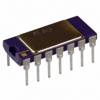
IC TRUE RMS/DC CONV 14-CDIP

AD536AKD

Manufacturer Part Number
AD536AKD
Description
IC TRUE RMS/DC CONV 14-CDIP
Manufacturer
Analog Devices Inc
Datasheet

Specifications of AD536AKD

Rohs Status
RoHS non-compliant
Current - Supply
1.2mA
Voltage - Supply
5.0V ~ 36V, ±3.0V ~ 18V
Mounting Type
Through Hole
Package / Case
14-CDIP (0.300", 7.62mm)
Accuracy %
0.2%
Bandwidth
450kHz
Supply Current
1.2mA
Power Dissipation Pd
500mW
Supply Voltage Range
5V To 36V
Digital Ic Case Style
DIP
No. Of Pins
14
Lead Free Status / RoHS Status
Contains lead / RoHS non-compliant

Available stocks

Company
Part Number
Manufacturer
Quantity
Price
Part Number:
AD536AKD
Manufacturer:
ADI
Quantity:
754
Part Number:
AD536AKD
Manufacturer:
INTEL
Quantity:
2 390
Part Number:
AD536AKD
Manufacturer:
ADI
Quantity:
358
Part Number:
AD536AKD
Manufacturer:
ADI/亚德诺
Quantity:
20 000
Part Number:
AD536AKDZ
Manufacturer:
Analog Devices Inc
Quantity:
135
Part Number:
AD536AKDZ
Manufacturer:
ADI
Quantity:
358
FEATURES
True rms-to-dc conversion
Laser trimmed to high accuracy
Wide response capability
dB output with 60 dB range
Low power: 1.2 mA quiescent current
Single- or dual-supply operation
Monolithic integrated circuit
−55°C to +125°C operation (AD536AS)
GENERAL DESCRIPTION
The AD536A is a complete monolithic integrated circuit that
performs true rms-to-dc conversion. It offers performance
comparable or superior to that of hybrid or modular units costing
much more. The AD536A directly computes the true rms value of
any complex input waveform containing ac and dc components.
A crest factor compensation scheme allows measurements with 1%
error at crest factors up to 7. The wide bandwidth of the device
extends the measurement capability to 300 kHz with less than 3 dB
errors for signal levels greater than 100 mV.
An important feature of the AD536A, not previously available
in rms converters, is an auxiliary dB output pin. The logarithm
of the rms output signal is brought out to a separate pin to allow
the dB conversion, with a useful dynamic range of 60 dB. Using
an externally supplied reference current, the 0 dB level can be
conveniently set to correspond to any input level from 0.1 V to
2 V rms.
The AD536A is laser trimmed to minimize input and output offset
voltage, to optimize positive and negative waveform symmetry
(dc reversal error), and to provide full-scale accuracy at 7 V rms.
As a result, no external trims are required to achieve the rated
unit accuracy.
The input and output pins are fully protected. The input circuitry
can take overload voltages well beyond the supply levels. Loss of
supply voltage with the input connected to external circuitry does
not cause the device to fail. The output is short-circuit protected.
Rev. D
Information furnished by Analog Devices is believed to be accurate and reliable. However, no
responsibility is assumed by Analog Devices for its use, nor for any infringements of patents or other
rights of third parties that may result from its use. Specifications subject to change without notice. No
license is granted by implication or otherwise under any patent or patent rights of Analog Devices.
Trademarks and registered trademarks are the property of their respective owners.
±0.2% maximum error (AD536AK)
±0.5% maximum error (AD536AJ)
Computes rms of ac and dc signals
450 kHz bandwidth: V rms > 100 mV
2 MHz bandwidth: V rms > 1 V
Signal crest factor of 7 for 1% error
One Technology Way, P.O. Box 9106, Norwood, MA 02062-9106, U.S.A.
Tel: 781.329.4700
Fax: 781.461.3113
The AD536A is available in two accuracy grades (J and K) for
commercial temperature range (0°C to 70°C) applications, and
one grade (S) rated for the −55°C to +125°C extended range.
The AD536AK offers a maximum total error of ±2 mV ± 0.2%
of reading, while the AD536AJ and AD536AS have maximum
errors of ±5 mV ± 0.5% of reading. All three versions are available
in a hermetically sealed 14-lead DIP or a 10-pin TO-100 metal
header package. The AD536AS is also available in a 20-terminal
leadless hermetically sealed ceramic chip carrier.
The AD536A computes the true root-mean-square level of a
complex ac (or ac plus dc) input signal and provides an equiva-
lent dc output level. The true rms value of a waveform is a more
useful quantity than the average rectified value because it relates
directly to the power of the signal. The rms value of a statistical
signal also relates to its standard deviation.
An external capacitor is required to perform measurements to
the fully specified accuracy. The value of this capacitor deter-
mines the low frequency ac accuracy, ripple amplitude, and
settling time.
The AD536A operates equally well from split supplies or a
single supply with total supply levels from 5 V to 36 V. With
1 mA quiescent supply current, the device is well suited for a
wide variety of remote controllers and battery-powered
instruments.
True RMS-to-DC Converter
+V
S
FUNCTIONAL BLOCK DIAGRAM
BUF IN
+
C
V
AV
IN
©1976–2008 Analog Devices, Inc. All rights reserved.
Integrated Circuit
Figure 1.
ABSOLUTE
SQUARER/
AD536A
CURRENT
DIVIDER
MIRROR
VALUE
BUF
25kΩ
25kΩ
AD536A
www.analog.com
dB
R
I
BUF
OUT
OUT
L

Related parts for AD536AKD

AD536AKD Summary of contents

Page 1

FEATURES True rms-to-dc conversion Laser trimmed to high accuracy ±0.2% maximum error (AD536AK) ±0.5% maximum error (AD536AJ) Wide response capability Computes rms of ac and dc signals 450 kHz bandwidth: V rms > 100 mV 2 MHz bandwidth: V rms ...

Page 2

AD536A TABLE OF CONTENTS Features .............................................................................................. 1 General Description ......................................................................... 1 Functional Block Diagram .............................................................. 1 Revision History ............................................................................... 2 Specifications ..................................................................................... 3 Absolute Maximum Ratings ............................................................ 5 ESD Caution .................................................................................. 5 Pin Configurations and Function Descriptions ........................... 6 Applications ...

Page 3

SPECIFICATIONS T = +25°C and ±15 V dc, unless otherwise noted. A Table 1. AD536AJ Parameter Min Typ TRANSFER FUNCTION V OUT CONVERSION ACCURACY 1 Total Error, Internal Trim (See Figure 6) vs. Temperature T to +70°C MIN +70°C to ...

Page 4

AD536A AD536AJ Parameter Min Typ I TERMINAL OUT I Scale Factor 40 OUT I Scale Factor Tolerance ±10 OUT Output Resistance 20 25 Voltage Compliance −V (+V BUFFER AMPLIFIER Input and Output Voltage − Range (+V − 2.5V) ...

Page 5

ABSOLUTE MAXIMUM RATINGS Table 2. Parameter Supply Voltage Dual Supply Single Supply Internal Power Dissipation Maximum Input Voltage Buffer Maximum Input Voltage Maximum Input Voltage Storage Temperature Range Operating Temperature Range AD536AJ/AD536AK AD536AS Lead Temperature (Soldering, 60 sec) ESD Rating ...

Page 6

AD536A PIN CONFIGURATIONS AND FUNCTION DESCRIPTIONS Table 3. D-14 and Q-14 Packages Pin Function Descriptions Pin No. Mnemonic − BUF OUT 7 BUF OUT ...

Page 7

Table 5. E-20 Package Pin Function Descriptions Pin No. Mnemonic − BUF OUT 10 BUF OUT ...

Page 8

AD536A APPLICATIONS INFORMATION TYPICAL CONNECTIONS The AD536A is simple to connect to for the majority of high accuracy rms measurements, requiring only an external capaci- tor to set the averaging time constant. The standard connection is shown in Figure 6 ...

Page 9

C AV SCALE FACTOR ADJUST V IN ABSOLUTE VALUE R1 AD536A 500Ω –V SQUARER/ S – DIVIDER CURRENT MIRROR BUF OUT V 6 ...

Page 10

AD536A The primary disadvantage in using a large C is that the settling time for a step change in input level is increased proportionately. Figure 12 illustrates that the relationship between C and 1% settling time is 115 ms for ...

Page 11

THEORY OF OPERATION The AD536A embodies an implicit solution of the rms equation that overcomes the dynamic range as well as other limitations inherent in a straightforward computation of rms. The actual computation performed by the AD536A follows the equation ...

Page 12

AD536A –V S – C1 0.1µF BUF OUT 6 dB OUT BUF IN 3mV/ SPECIAL TC COMPENSATION RESISTOR, +3300 ...

Page 13

OUT 5 0 ±6 ±10 VOLTS (DUAL SUPPLY) Figure 21. Input and Output Voltage Ranges vs. Dual Supply 2.5 0 ±16 ±18 Figure 22. Input and Output Voltage ...

Page 14

AD536A OUTLINE DIMENSIONS 0.358 (9.09) 0.342 (8.69) CONTROLLING DIMENSIONS ARE IN INCHES; MILLIMETER DIMENSIONS (IN PARENTHESES) ARE ROUNDED-OFF INCH EQUIVALENTS FOR REFERENCE ONLY AND ARE NOT APPROPRIATE FOR USE IN DESIGN. 0.005 (0.13) MIN 0.080 (2.03) MAX 14 8 0.310 ...

Page 15

... REFERENCE ONLY AND ARE NOT APPROPRIATE FOR USE IN DESIGN. ORDERING GUIDE Model Temperature Range AD536AJD 0°C to +70°C 1 AD536AJDZ 0°C to +70°C AD536AKD 0°C to +70°C 1 AD536AKDZ 0°C to +70°C AD536AJH 0°C to +70°C AD536AJHZ 1 0°C to +70°C AD536AKH 0°C to +70°C AD536AKHZ 1 0°C to +70°C AD536AJQ 0° ...

Page 16

AD536A NOTES ©1976–2008 Analog Devices, Inc. All rights reserved. Trademarks and registered trademarks are the property of their respective owners. D00504-0-8/08(D) Rev Page ...

Related keywords