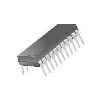
KA3511DS Fairchild Semiconductor, KA3511DS Datasheet - Page 7

KA3511DS
Manufacturer Part Number
KA3511DS
Description
IC PWM/SECONDARY COMBO 22-DIP
Manufacturer
Fairchild Semiconductor
Datasheet
1.KA3511DS.pdf
(28 pages)
Specifications of KA3511DS
Pwm Type
Current Mode
Number Of Outputs
3
Frequency - Max
10kHz
Duty Cycle
50%
Voltage - Supply
14 V ~ 30 V
Buck
No
Boost
No
Flyback
No
Inverting
No
Doubler
No
Divider
No
Cuk
No
Isolated
No
Operating Temperature
-25°C ~ 85°C
Package / Case
22-DIP (0.400", 10.16mm)
Frequency-max
10kHz
Topology
Push-Pull
Output Voltage
40 V
Output Current
200 mA
Switching Frequency
10 KHz
Maximum Operating Temperature
+ 85 C
Minimum Operating Temperature
- 25 C
Fall Time
50 ns
Mounting Style
Through Hole
Rise Time
100 ns
Synchronous Pin
No
Lead Free Status / RoHS Status
Lead free / RoHS Compliant
Available stocks
Company
Part Number
Manufacturer
Quantity
Price
Company:
Part Number:
KA3511DS
Manufacturer:
NMB
Quantity:
2 000
5. ELECTRICAL CHARACTERISTICS (continued)
Notes:
1. These Parameters, although guaranteed over their recommended operating conditions are not 100%
2. REM on delay time (Pin6 REM: “L”
Over voltage protection for 5V
Over voltage protection for 12V
Input threshold voltage for PT
Under voltage protection for 3.3V
Under voltage protection for 5V
Under voltage protection for 12V
Charging current for UVP delay
UVP Delay Time
REMOTE ON/OFF SECTION
REM on input voltage
REM off input voltage
REM off input bias voltage
REM on open voltage
REM on delay time
REM off delay time
REMOTE ON/OFF SECTION
Detecting input voltage
Detecting V5 voltage
Hysteresis voltage 1
Hysteresis voltage 2
PG output load resistor
Charging current for PG delay
PG delay time
PG output saturation voltage
TOTAL DEVICE
Standby supply current
tested in production.
REM off delay time (Pin6 REM: “H”
Characteristic
(2)
V
“H”),
I
REM(OPEN)
V
“L”)
Symbol
V
I
CHG.UVP
V
T
V
V
V
V
CHG.PG
V
V
V
I
T
SAT(PG)
IN(DET)
D.UVP
REML
5(DET)
HY1
HY2
R
V
REMH
REML
Ton
Toff
OVP2
OVP3
UVP1
UVP2
UVP3
I
D.PG
CC
PG
PT
7
C=2.2µF, V
C=2.2µF
I
V
C=0.1µF
C=0.1µF
COMP1, 2
COMP3
C=2.2µF, V
C=2.2µF
I
REM
PG
REM
Test Condition
=10mA
= -200µA
=0.4V
–
–
–
–
–
–
–
–
–
–
–
–
TH
TH
=1.8V
=1.8V
Min. Typ. Max.
13.5 14.2 15.0
1.20 1.25 1.30
1.20 1.25 1.30
100
100
-10
-10
5.8
2.1
3.7
9.2
2.0
2.0
4.1
0.6
0.5
16
10
–
–
4
–
–
Value
260
260
6.2
2.3
4.0
-15
4.3
1.2
-15
0.4
10
24
40
10
Rev C, November 1999
–
–
–
–
8
1
10.8
5.25
-1.6
500
500
6.6
2.5
4.3
-23
0.8
4.5
-23
0.2
14
34
80
20
–
–
2
Unit
mA
mV
mA
ms
ms
ms
ms
uA
k
uA
V
V
V
V
V
V
V
V
V
V
V
V


