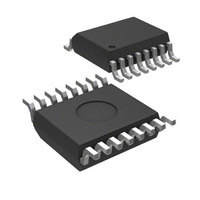
MIC2186BQS Micrel Inc, MIC2186BQS Datasheet - Page 2

MIC2186BQS
Manufacturer Part Number
MIC2186BQS
Description
IC PWM BST FLYBCK CM 16QSOP
Manufacturer
Micrel Inc
Datasheet
1.MIC2186YM.pdf
(15 pages)
Specifications of MIC2186BQS
Pwm Type
Current Mode
Number Of Outputs
1
Frequency - Max
440kHz
Duty Cycle
85%
Voltage - Supply
2.9 V ~ 14 V
Buck
No
Boost
Yes
Flyback
Yes
Inverting
No
Doubler
No
Divider
No
Cuk
No
Isolated
No
Operating Temperature
-40°C ~ 125°C
Package / Case
16-QSOP
Frequency-max
440kHz
Lead Free Status / RoHS Status
Contains lead / RoHS non-compliant
MIC2186
Pin Configuration
Pin Description
M9999-042205
Pin Number
10
11
12
13
14
15
16
1
2
3
4
5
6
7
8
9
Pin Name
EN/UVLO
FREQ/2
COMP
SGND
PGND
SYNC
OUTN
VREF
VINA
HIDC
VINP
SKIP
CSH
VDD
SS
FB
EN/UVLO
16-pin Narrow Body SOP (M)
COMP
SGND
VREF
VINA
SKIP
SS
FB
Pin Function
Input voltage to control circuitry (2.9V to 14V).
SKIP (Input): Regulator operates in PWM mode (no pulse skipping) when
pin is pulled low, and skip mode when raised to Vdd. There is no automatic
switching between PWM and skip mode available on this device.
Soft start reduces the inrush current and delays and slows the output voltage
rise time. A 5µA current source will charge the capacitor up to Vdd.
Compensation (Output): Internal error amplifier output. Connect to a
capacitor or series RC network to compensate the regulator’s control loop.
Small signal ground: must be routed separately from other grounds to the (-)
terminal of Cout.
Feedback Input - regulates FB to 1.245V.
Enable/Undervoltage Lockout (input): A low level on this pin will power down
the device, reducing the quiescent current to under 0.5µA. This pin has two
separate thresholds, below 1.5V the output switching is disabled, and below
0.9V the device is forced into a complete micropower shutdown. The 1.5V
threshold functions as an accurate undervoltage lockout (UVLO) with 135mV
hysteresis.
The 1.245V reference is available on this pin. A 0.1µF capacitor should be
connected form this pin to SGnd.
The (+) input to the current limit comparator. A built in offset of 100mV
between CSH and SGnd in conjunction with the current sense resistor sets
the current limit threshold level. This is also the (+) input to the current
amplifier.
3V internal linear-regulator output. Vdd is also the supply voltage bus for the
chip. Bypass to SGND with 1µF. Maximum source current is 0.5mA.
Frequency Synchronization (Input): Connect an external clock signal to
synchronize the oscillator. Leading edge of signal above 1.5V starts switch-
ing cycle. Connect to SGND if not used.
MOSFET driver power ground, connects to the bottom of the current sense
resistor and the (–) terminal of C
High Duty Cycle. Sets duty cycle and frequency along with Freq/2. Logic
HIGH sets 85% maximum duty cycle. Logic LOW sets 50% maximum duty
cycle. See applications section for more information.
High current drive for N channel MOSFET. Voltage swing is from ground to
V
Sets duty cycle and frequency along with HiDC. See applications section for
more information.
Power input voltage to the gate drive circuitry (2.9V to 14V). This pin is
normally connected to the output voltage.
16-pin QSOP (QS)
IN
. R
1
2
3
4
5
6
7
8
ON
is typically 1.6Ω.
2
16 VINP
15
14
13
12
11
10
9
FREQ/2
OUTN
HIDC
PGND
SYNC
VDD
CSH
IN
.
Micrel, Inc.
April 2005


