ISL6265HRTZ Intersil, ISL6265HRTZ Datasheet
ISL6265HRTZ
Specifications of ISL6265HRTZ
Available stocks


Related parts for ISL6265HRTZ

ISL6265HRTZ Summary of contents
Page 1
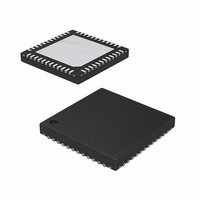
... TEMP (°C) ISL6265HRTZ ISL6265 HRTZ -10 to +100 48 Ld 6x6 TQFN L48.6x6 ISL6265HRTZ-T* ISL6265 HRTZ -10 to +100 48 Ld 6x6 TQFN * Please refer to TB347 for details on reel specifications. NOTE: These Intersil Pb-free plastic packaged products employ special Pb-free material sets; molding compounds/die attach materials and 100% ...
Page 2
Function Block Diagram RTN_NB SVC NO DROOP SVD PSI_L I_OFS PWROK VREF_NB VREF0 VREF1 OFS/FIXEN OCSET_NB OCSET RBIAS VW0 COMP0 FB0 VDIFF0 V0 VSEN0 1 RTN0 DROOP ISP0 CURRENT SENSE ISN0 ISP1 CURRENT SENSE ISN1 V1 VSEN1 1 RTN1 VDIFF1 ...
Page 3
Simplified Application Circuit for Dual Plane and Northbridge Support SVI DATA SVI CLOCK ENABLE PWROK VDDPWRGD REMOTE SENSE REMOTE SENSE VDD_PLANE_STRAP FIGURE 2. ISL6265 BASED DUAL-PLANE AND NORTHBRIDGE CONVERTERS WITH INDUCTOR DCR CURRENT SENSING 3 ISL6265 VIN +5V VIN VCC ...
Page 4
Simplified Application Circuit for Uniplane Core and Northbridge Support +5V SVI DATA SVD SVI CLOCK SVC ENABLE EN PWROK PWROK VDDPWRGD PGOOD VSEN0 REMOTE SENSE RTN0 REMOTE VSEN1 SENSE VDD_PLANE_STRAP RTN1 OFS/VFIXEN VDIFF0 FB0 COMP0 VW0 VDIFF1 OPEN OPEN FB1 ...
Page 5
Simplified Application Circuit for Dual Layout +5V SVI DATA SVD SVI CLOCK SVC ENABLE EN PWROK PWROK VDDPWRGD PGOOD VSEN0 REMOTE SENSE RTN0 VDD_PLANE_STRAP DNP DUAL PLANE RTN1 REMOTE DNP UNIPLANE SENSE VSEN1 OFS/VFIXEN VDIFF0 FB0 COMP0 VW0 VDIFF1 FB1 ...
Page 6
... Thermal Resistance (Typical, Notes 1, 2) θ TQFN Package . . . . . . . . . . . . . . . . . . Maximum Junction Temperature . . . . . . . . . . . . . . . . . . . . . . +150°C Maximum Storage Temperature Range . . . . . . . . . .-65°C to +150°C Pb-free reflow profile . . . . . . . . . . . . . . . . . . . . . . . . . .see link below http://www.intersil.com/pbfree/Pb-FreeReflow.asp Recommended Operating Conditions Supply Voltage, VCC, PVCC . . . . . . . . . . . . . . . . . . . . . . . .+5V ±5% Battery Voltage, VIN . . . . . . . . . . . . . . . . . . . . . . . . . . . . +6V to 24V Ambient Temperature . . . . . . . . . . . . . . . . . . . . . . .-10°C to +100°C Junction Temperature . . . . . . . . . . . . . . . . . . . . . . .-10° ...
Page 7
Electrical Specifications VCC = PVCC = 5V +25°C, unless otherwise specified. Temperature limits established by characterization and are not production tested. (Continued) PARAMETER CORE CURRENT SENSE (Note 3) Current Imbalance Threshold Input Bias Current RTN1 Threshold SOFT START/VID-ON-THE-FLY ...
Page 8
Electrical Specifications VCC = PVCC = 5V +25°C, unless otherwise specified. Temperature limits established by characterization and are not production tested. (Continued) PARAMETER OFFSET FUNCTION OFS Pin Voltage For Droop Enabling FB Pin Source Current OFS Pin Voltage ...
Page 9
Functional Pin Description OFS/VFIXEN 1 PGOOD 2 PWROK 3 SVD 4 SVC 5 ENABLE 49 6 GND RBIAS 7 OCSET 8 VDIFF_0 9 FB_0 10 COMP_0 11 VW0 ...
Page 10
... PWM while eliminating many of their shortcomings. The ISL6265 modulator internally synthesizes an analog of the inductor ripple current and uses hysteretic comparators on those signals to establish PWM pulse widths. Operating on these large-amplitude, noise-free synthesized signals allows the ISL6265 to achieve lower 3 Technology™, Intersil's 3 modulator FN6599.1 May 13, 2009 ...
Page 11
... Modulator The ISL6265 modulator features Intersil’s R hybrid of fixed frequency PWM control and variable frequency hysteretic control (see Figure 5). Intersil’s R technology can simultaneously affect the PWM switching frequency and PWM duty cycle in response to input voltage 3 and output load transients ...
Page 12
ENABLE. If RTN1 is low prior to ENABLE, both VDD0 and VDD1 core planes are required. The core controllers operate as independent single-phase regulators. RTN1 is connected to the CPU Core1 negative sense point. For single core CPU designs (uniplane), ...
Page 13
ISL6265 decodes and locks the decoded value in an on-board hold register. TABLE 1. PRE-PWROK METAL VID CODES SVC SVD OUTPUT VOLTAGE ( The internal DAC circuitry begins to ramp ...
Page 14
SVI WIRE Protocol The SVI wire protocol is based on the I wires (serial clock (SVC) and serial data (SVD)), carry information between the AMD processor (master) and VR controller (slave) on the bus. The master initiates and terminates SVI ...
Page 15
SVC SVD SLAVE ADDRESS PHASE SVI Bus Protocol The AMD processor bus protocol is compliant with SMBus send byte protocol for VID transactions (see Figure 8). During a send byte transaction, the processor sends the start sequence ...
Page 16
Estimating the value written as shown in FSET_NB Equation -------------------- - = ⋅ FSET Where F is the PWM switching frequency the programming resistor and K = 1.5 x ...
Page 17
AMD specifications do not require droop and provide no load line guidelines. Tight static output voltage tolerance limits push acceptable level of droop below a useful level for Griffin applications. Care must be taken in applications which implement droop to ...
Page 18
In DE, the ISL6265 Core regulators automatically enter DCM after the PHASE pin has detected positive voltage and LGATE was allowed to go high. The NB regulator enters DCM after the PHASE pin has detected positive voltage ...
Page 19
CURRENT ADDITIONAL DETAIL SENSE ISP 5x ISN C(OC TRIP CURRENT BIAS CKT OC - OCSET + 6 V OCSET 6 ISL6265 FIGURE 10. OC TRIP CIRCUITRY The sense capacitor voltage will increase ...
Page 20
... It is assumed that the reader is familiar with many of the basic skills and techniques referenced in the following section. In addition to this guide, Intersil provides complete reference designs that include schematics, bills of materials, and example board layouts. ...
Page 21
P-P,N P-P,N 0.55 0.50 0.45 0. P-P,N 0.35 0. 0.25 P-P,N 0.25 0.20 0.15 0.10 0. 0.1 0.2 0.3 0.4 0.5 0.6 DUTY CYCLE (V FIGURE 11. NORMALIZED ...
Page 22
The bootstrap capacitor must have a maximum voltage rating above PVCC + 4V and its capacitance value is selected per Equation 27 ≥ C ----------------------- - ΔV BOOT BOOT Where the total gate charge required ...
Page 23
... Accordingly, the reader is cautioned to verify that data sheets are current before placing orders. Information furnished by Intersil is believed to be accurate and reliable. However, no responsibility is assumed by Intersil or its subsidiaries for its use; nor for any infringements of patents or other rights of third parties which may result from its use ...
Page 24
Package Outline Drawing L48.6x6 48 LEAD THIN QUAD FLAT NO-LEAD PLASTIC PACKAGE Rev 1, 4/07 6.00 6 PIN 1 INDEX AREA (4X) 0.15 TOP VIEW ( 5. 75 TYP ) ( TYPICAL RECOMMENDED LAND PATTERN 24 ISL6265 ...