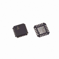
HIP6004BCR Intersil, HIP6004BCR Datasheet - Page 8

HIP6004BCR
Manufacturer Part Number
HIP6004BCR
Description
IC CTRLR PWM VOLTAGE MON 20-QFN
Manufacturer
Intersil
Datasheet
1.HIP6004BCBZA.pdf
(15 pages)
Specifications of HIP6004BCR
Applications
Controller, Intel Pentium®, II, Pro
Voltage - Input
5V, 12V
Number Of Outputs
1
Voltage - Output
1.3 ~ 3.5 V
Operating Temperature
0°C ~ 70°C
Mounting Type
Surface Mount
Package / Case
20-TQFN Exposed Pad
Lead Free Status / RoHS Status
Contains lead / RoHS non-compliant
NOTE: 0 = connected to GND or V
Figure 5 shows the critical power components of the converter.
To minimize the voltage overshoot the interconnecting wires
indicated by heavy lines should be part of ground or power
plane in a printed circuit board. The components shown in
Figure 5 should be located as close together as possible.
Please note that the capacitors C
numerous physical capacitors. Locate the HIP6004B within 3
inches of the MOSFETs, Q
MOSFETs’ gate and source connections from the HIP6004B
must be sized to handle up to 1A peak current.
Figure 6 shows the circuit traces that require additional
layout consideration. Use single point and ground plane
construction for the circuits shown. Minimize any leakage
VID4
FIGURE 5. PRINTED CIRCUIT BOARD POWER AND
0
0
0
0
0
0
0
0
0
0
0
0
0
0
0
0
HIP6004B
VID3
UGATE
PHASE
LGATE
PGND
1
1
1
1
1
1
1
1
0
0
0
0
0
0
0
0
GROUND PLANES OR ISLANDS
PIN NAME
VID2
1
1
1
1
0
0
0
0
1
1
1
1
0
0
0
0
1
Q
V
Q
RETURN
VID1
and Q
2
IN
1
1
1
0
0
1
1
0
0
1
1
0
0
1
1
0
0
8
SS
IN
D
2
, 1 = connected to V
2
and C
. The circuit traces for the
VID0
1
0
1
0
1
0
1
0
1
0
1
0
1
0
1
0
C
O
IN
each represent
L
O
VOLTAGE DACOUT
NOMINAL OUTPUT
TABLE 1. OUTPUT VOLTAGE PROGRAM
C
O
V
OUT
1.30
1.35
1.40
1.45
1.50
1.55
1.60
1.65
1.70
1.75
1.80
1.85
1.90
1.95
2.00
2.05
DD
through pull-up resistors.
HIP6004B
VID4
1
1
1
1
1
1
1
1
1
1
1
1
1
1
1
1
current paths on the SS PIN and locate the capacitor, C
close to the SS pin because the internal current source is
only 10µA. Provide local V
GND pins. Locate the capacitor, C
practical to the BOOT and PHASE pins.
Feedback Compensation
Figure 7 highlights the voltage-mode control loop for a
synchronous-rectified buck converter. The output voltage
(V
error amplifier (Error Amp) output (V
the oscillator (OSC) triangular wave to provide a pulse-
width modulated (PWM) wave with an amplitude of V
the PHASE node.
C
OUT
SS
FIGURE 6. PRINTED CIRCUIT BOARD SMALL SIGNAL
SS
VID3
) is regulated to the Reference voltage level. The
1
1
1
1
1
1
1
1
0
0
0
0
0
0
0
0
HIP6004B
PIN NAME
GND
LAYOUT GUIDELINES
VID2
1
1
1
1
0
0
0
0
1
1
1
1
0
0
0
0
BOOT
PHASE
V
C
CC
VID1
BOOT
1
1
0
0
1
1
0
0
1
1
0
0
1
1
0
0
CC
+12V
decoupling between V
C
D
VCC
VID0
1
1
0
1
0
1
0
1
0
1
0
1
0
1
0
1
0
BOOT
E/A
VOLTAGE DACOUT
) is compared with
NOMINAL OUTPUT
as close as
Q
+V
Q
1
2
IN
L
O
C
2.1
2.2
2.3
2.4
2.5
2.6
2.7
2.8
2.9
3.0
3.1
3.2
3.3
3.4
3.5
O
0
CC
IN
V
SS
and
OUT
at


