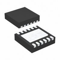
LTC3535EDD#PBF Linear Technology, LTC3535EDD#PBF Datasheet - Page 9

LTC3535EDD#PBF
Manufacturer Part Number
LTC3535EDD#PBF
Description
IC DC/DC CONV 550MA DL 12-DFN
Manufacturer
Linear Technology
Type
Step-Up (Boost)r
Datasheet
1.LTC3535EDDPBF.pdf
(16 pages)
Specifications of LTC3535EDD#PBF
Internal Switch(s)
Yes
Synchronous Rectifier
Yes
Number Of Outputs
2
Voltage - Output
1.5 ~ 5.25 V
Current - Output
550mA
Frequency - Switching
1MHz
Voltage - Input
0.5 ~ 5 V
Operating Temperature
-40°C ~ 85°C
Mounting Type
Surface Mount
Package / Case
12-DFN
Primary Input Voltage
6V
No. Of Outputs
2
Output Voltage
5.25V
Output Current
550mA
No. Of Pins
12
Operating Temperature Range
-40°C To +85°C
Msl
MSL 1 - Unlimited
Rohs Compliant
Yes
Lead Free Status / RoHS Status
Lead free / RoHS Compliant
Power - Output
-
Available stocks
Company
Part Number
Manufacturer
Quantity
Price
OPERATION
The LTC3535 is a dual channel 1MHz synchronous boost
converter housed in a 12-lead 3mm × 3mm DFN package.
Each channel is identical and fully independent. They can
operate from the same source, or from different voltage
sources.
In addition, their output voltages can be tied together
to allow operation of a single output from two different
input sources. However, note that the two channels are
not designed to current share, so if both input voltages
are present either one may be supplying the load.
The following description of operation applies to each
channel. Note that references to V
corresponding channel.
With a guaranteed ability to start up and operate from
inputs less than 0.8V, each channel features fixed fre-
quency, current mode PWM control for exceptional line
and load regulation. The current mode architecture with
adaptive slope compensation provides excellent transient
load response, requiring minimal output filtering. Internal
soft-start and internal loop compensation simplifies the
design process while minimizing the number of external
components.
With its low R
MOSFET switch and P-channel MOSFET synchronous
rectifier, the LTC3535 achieves high efficiency over a wide
range of load currents. Burst Mode operation maintains
high efficiency at very light loads, reducing the quiescent
current to just 9µA per channel. Operation can be best
understood by referring to the Block Diagram.
LOW VOLTAGE START-UP
The LTC3535 includes an independent start-up oscillator
designed to start up at an input voltage of 0.68V (typical).
Soft-start and inrush current limiting are provided during
start-up, as well as normal mode.
When either V
typical, the channel enters normal operating mode. When
DS(ON)
IN
or V
and low gate charge internal N-channel
OUT
(Refer to Block Diagram)
for a given channel exceeds 1.3V
IN
or V
OUT
apply to the
the output voltage exceeds the input by 0.24V, the channel
powers itself from V
internal circuitry has no dependency on the V
age, eliminating the requirement for a large input capacitor.
The input voltage can drop as low as 0.5V. The limiting
factor for the application becomes the availability of the
power source to supply sufficient energy to the output at
low voltages, and maximum duty cycle, which is clamped at
90% typical. Note that at low input voltages, small voltage
drops due to series resistance become critical, and greatly
limit the power delivery capability of the converter.
LOW NOISE FIXED FREQUENCY OPERATION
Soft-Start
The LTC3535 contains internal circuitry to provide soft-
start operation. The soft-start circuitry slowly ramps the
peak inductor current from zero to its peak value of 750mA
(typical) in approximately 0.5ms, allowing start-up into
heavy loads. The soft-start circuitry is reset in the event
of a shutdown command or a thermal shutdown.
Oscillator
An internal oscillator (independent for each channel) sets
the switching frequency to 1MHz.
Shutdown
Shutdown is accomplished by pulling the SHDN pin below
0.3V and enabled by pulling the SHDN pin above 0.8V.
Although SHDN can be driven above V
absolute maximum rating) without damage, the LTC3535
has a proprietary test mode that may be engaged if SHDN
is held in the range of 0.5V to 1V higher than the greater
of V
switching action is interrupted, which can cause undesir-
able operation in some applications. Therefore, in appli-
cations where SHDN may be driven above V
divider or other means must be employed to keep the SHDN
voltage below (V
IN
or V
OUT
. If the test mode is engaged, normal PWM
IN
+ 0.4V) to prevent the possibility of
OUT
instead of V
IN
IN
. At this point the
LTC3535
or V
OUT
IN
IN
, a resistor
input volt-
(up to the
3535fa
9


