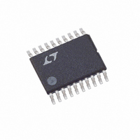
LTC3778EF#PBF Linear Technology, LTC3778EF#PBF Datasheet - Page 10

LTC3778EF#PBF
Manufacturer Part Number
LTC3778EF#PBF
Description
IC STEP-DWN CONTRLR SYNC 20TSSOP
Manufacturer
Linear Technology
Type
Step-Down (Buck)r
Datasheet
1.LTC3778EFPBF.pdf
(24 pages)
Specifications of LTC3778EF#PBF
Internal Switch(s)
No
Synchronous Rectifier
Yes
Number Of Outputs
1
Voltage - Output
0.6 ~ 32.4 V
Current - Output
2A
Frequency - Switching
Adjustable
Voltage - Input
4 ~ 36 V
Operating Temperature
-40°C ~ 85°C
Mounting Type
Surface Mount
Package / Case
20-TSSOP
Primary Input Voltage
36V
No. Of Outputs
1
Output Voltage
36V
Output Current
2A
No. Of Pins
20
Operating Temperature Range
-40°C To +85°C
Msl
MSL 1 - Unlimited
Rohs Compliant
Yes
Lead Free Status / RoHS Status
Lead free / RoHS Compliant
Power - Output
-
Available stocks
Company
Part Number
Manufacturer
Quantity
Price
APPLICATIO S I FOR ATIO
LTC3778
The basic LTC3778 application circuit is shown in
Figure 1. External component selection is primarily de-
termined by the maximum load current and begins with
the selection of the sense resistance and power MOSFET
switches. The LTC3778 can use either a sense resistor or
the on-resistance of the synchronous power MOSFET for
determining the inductor current. The desired amount of
ripple current and operating frequency largely deter-
mines the inductor value. Finally, C
ability to handle the large RMS current into the converter
and C
output voltage ripple and transient specification.
Maximum Sense Voltage and V
Inductor current is determined by measuring the voltage
across a sense resistance that appears between the SENSE
and SENSE
the voltage applied to the V
approximately (0.133)V
loop will not allow the inductor current valleys to exceed
(0.133)V
margin for variations in the LTC3778 and external compo-
nent values and a good guide for selecting the sense
resistance is:
An external resistive divider from INTV
set the voltage of the V
resulting in nominal sense voltages of 50mV to 200mV.
Additionally, the V
in which case the nominal sense voltage defaults to 70mV
or 140mV, respectively. The maximum allowed sense
voltage is about 1.33 times this nominal value.
10
R
SENSE
OUT
RNG
is chosen with low enough ESR to meet the
+
/R
pins. The maximum sense voltage is set by
10 •
SENSE
I
V
OUT MAX
RNG
U
RNG
. In practice, one should allow some
(
pin can be tied to SGND or INTV
RNG
RNG
U
)
. The current mode control
pin between 0.5V and 2V
RNG
RNG
W
pin and is equal to
IN
Pin
is selected for its
CC
can be used to
U
CC
–
Connecting the SENSE
The LTC3778 can be used with or without a sense resistor.
When using a sense resistor, it is placed between the
source of the bottom MOSFET, M2, and PGND. Connect
the SENSE
sense resistor. Using a sense resistor provides a well
defined current limit, but adds cost and reduces efficiency.
Alternatively, one can eliminate the sense resistor and use
the bottom MOSFET as the current sense element by
simply connecting the SENSE
SENSE
must carefully choose the MOSFET on-resistance as dis-
cussed below.
Power MOSFET Selection
The LTC3778 requires two external N-channel power
MOSFETs, one for the top (main) switch and one for the
bottom (synchronous) switch. Important parameters for
the power MOSFETs are the breakdown voltage V
threshold voltage V
transfer capacitance C
The gate drive voltage is set by the 5V INTV
supplies. Consequently, logic-level threshold MOSFETs
must be used in LTC3778 applications. If the input voltage
or DRV
logic level threshold MOSFETs should be considered.
When the bottom MOSFET is used as the current sense
element, particular attention must be paid to its on-
resistance. MOSFET on-resistance is typically specified
with a maximum value R
additional margin is required to accommodate the rise in
MOSFET on-resistance with temperature:
R
DS ON MAX
(
–
CC
pin to PGND. This improves efficiency, but one
voltage is expected to drop below 5V, then sub-
)(
+
and SENSE
)
(GS)TH
R
SENSE
RSS
T
+
–
DS(ON)(MAX)
pins to the top and bottom of the
and SENSE
, on-resistance R
and maximum current I
+
pin to the SW pin and
at 25 C. In this case,
–
Pins
DS(ON)
CC
and DRV
, reverse
DS(MAX)
(BR)DSS
3778f
CC
,
.


