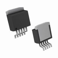
LM2585S-5.0/NOPB National Semiconductor, LM2585S-5.0/NOPB Datasheet - Page 3

LM2585S-5.0/NOPB
Manufacturer Part Number
LM2585S-5.0/NOPB
Description
IC MULTI CONFIG 5V 3A TO263-5
Manufacturer
National Semiconductor
Series
SIMPLE SWITCHER®r
Type
Step-Up (Boost), Flyback, Forward Converterr
Datasheet
1.LM2585T-ADJNOPB.pdf
(28 pages)
Specifications of LM2585S-5.0/NOPB
Internal Switch(s)
Yes
Synchronous Rectifier
No
Number Of Outputs
1
Voltage - Output
5V
Current - Output
3A
Frequency - Switching
100kHz
Voltage - Input
4 ~ 40 V
Operating Temperature
-40°C ~ 125°C
Mounting Type
Surface Mount
Package / Case
D²Pak, TO-263 (5 leads + tab)
For Use With
551011367-061 - BOARD WEBENCH LM2577,LM2585/87
Lead Free Status / RoHS Status
Lead free / RoHS Compliant
Power - Output
-
Other names
*LM2585S-5.0
*LM2585S-5.0/NOPB
LM2585S-5.0
*LM2585S-5.0/NOPB
LM2585S-5.0
SYSTEM PARAMETERS Test Circuit of
V
ΔV
ΔV
ΔV
ΔI
η
UNIQUE DEVICE PARAMETERS
V
ΔV
G
A
Symbol
OUT
REF
VOL
M
LOAD
Absolute Maximum Ratings
If Military/Aerospace specified devices are required,
please contact the National Semiconductor Sales Office/
Distributors for availability and specifications.
Electrical Characteristics
LM2585-3.3
Specifications with standard type face are for T
Range. Unless otherwise specified, V
Input Voltage
Switch Voltage
Switch Current
Compensation Pin Voltage
Feedback Pin Voltage
Storage Temperature Range
Lead Temperature
OUT
IN
OUT
REF
(Soldering, 10 sec.)
/
/
Output Voltage
Line Regulation
Load Regulation
Efficiency
Output Reference
Voltage
Reference Voltage
Line Regulation
Error Amp
Transconductance
Error Amp
Voltage Gain
(Note
Parameters
2)
(Note
V
I
V
I
V
I
V
Measured at Feedback Pin
V
V
I
V
V
R
−0.4V
LOAD
LOAD
LOAD
COMP
IN
IN
IN
IN
COMP
IN
COMP
COMP
COMP
IN
Figure 2 (Note
5)
−0.4V
= 4V to 12V
= 4V to 12V
= 12V
= 5V, I
= 4V to 40V
−0.4V
= 5V.
−0.4V
= 0.3A to 1.2A
= 0.3A
= 0.3A to 1.2A
= −30 μA to +30 μA
Internally Limited
−65°C to +150°C
= 1.0V
= 1.0V
= 0.5V to 1.6V
= 1.0 MΩ
≤
V
≤
LOAD
Conditions
J
COMP
≤
(Note
≤
V
= 25°C, and those in bold type face apply over full Operating Temperature
V
SW
V
IN
= 0.3A
FB
≤
260°C
≤
≤
(Note
1)
4)
≤
2.4V
45V
65V
2V
6)
3
Maximum Junction Temperature
(Note
Power Dissipation
Minimum ESD Rating
Supply Voltage
Output Switch Voltage
Output Switch Current
Junction Temperature Range
(C = 100 pF, R = 1.5 kΩ)
Typical
1.193
260
3.3
3.3
2.0
20
20
76
3)
3.242/3.234
(Note
3.17/3.14
Operating Ratings
151/75
0.678
Min
3)
3.358/3.366
−40°C
3.43/3.46
50/100
50/100
2.259
Max
Internally Limited
0V
4V
≤
≤
T
≤
www.national.com
V
J
I
SW
V
≤
SW
IN
+125°C
≤
150°C
≤
≤
mmho
Units
3.0A
2 kV
40V
60V
mV
mV
mV
V/V
%
V
V


